FAN6756 データシートの表示(PDF) - Fairchild Semiconductor
部品番号
コンポーネント説明
メーカー
FAN6756 Datasheet PDF : 18 Pages
| |||
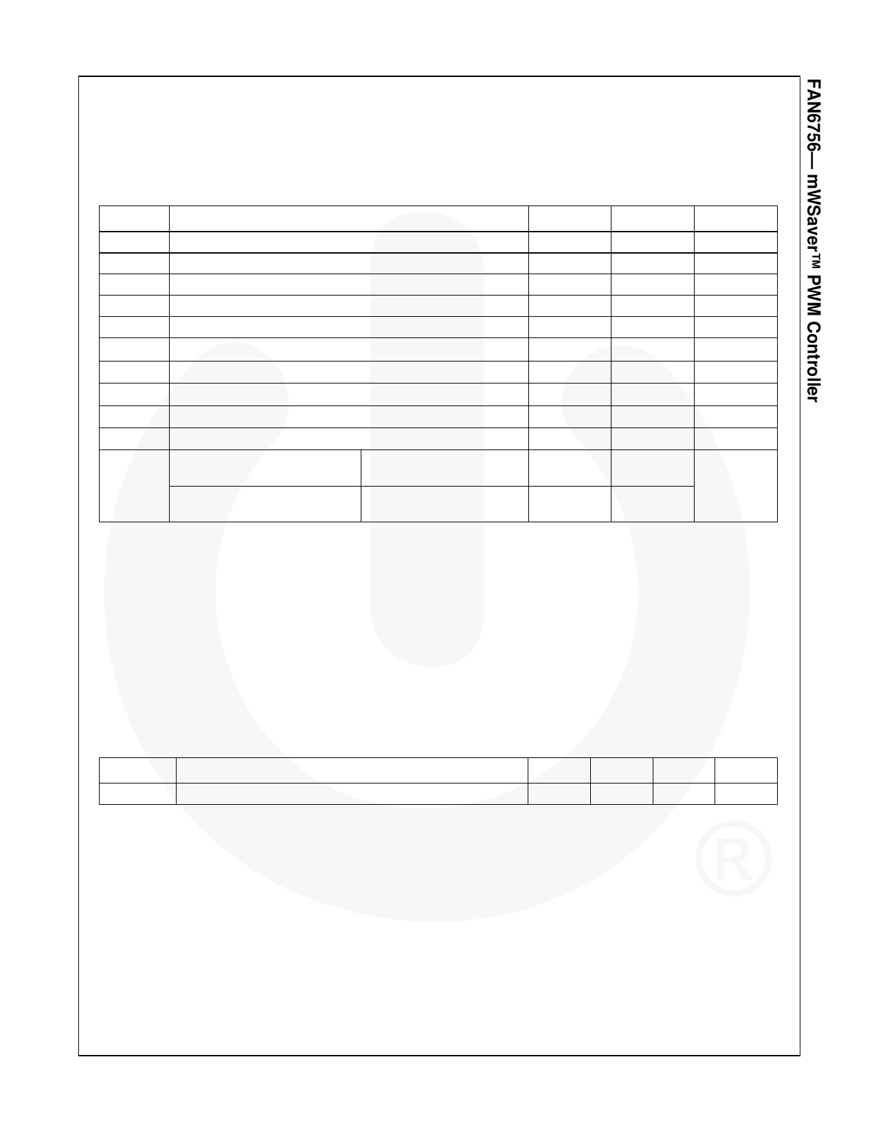
Absolute Maximum Ratings
Stresses exceeding the absolute maximum ratings may damage the device. The device may not function or be
operable above the recommended operating conditions and stressing the parts to these levels is not recommended.
In addition, extended exposure to stresses above the recommended operating conditions may affect device reliability.
The absolute maximum ratings are stress ratings only.
Symbol
Parameter
Min.
Max.
Unit
VVDD DC Supply Voltage(2,3)
30
V
VFB FB Pin Input Voltage
-0.3
7.0
V
VSENSE SENSE Pin Input Voltage
-0.3
7.0
V
VRT RT Pin Input Voltage
-0.3
7.0
V
VHV HV Pin Input Voltage
500
V
PD
Power Dissipation (TA<50°C)
400
mW
JA Thermal Resistance (Junction-to-Air)
150
C/W
TJ
Operating Junction Temperature
-40
+125
C
TSTG Storage Temperature Range
-55
+150
C
TL
Lead Temperature (Wave Soldering or IR, 10 Seconds)
+260
C
ESD
Human Body Model,
JEDEC:JESD22-A114
Charged Device Model,
JEDEC:JESD22-C101
All Pins Except HV Pin(4)
All Pins Except HV Pin(4)
6000
V
2000
Notes:
2. All voltage values, except differential voltages, are given with respect to the network ground terminal.
3. Stresses beyond those listed under Absolute Maximum Ratings may cause permanent damage to the device.
4. ESD level on HV pin is CDM=1250 V and HBM=500 V.
Recommended Operating Conditions
The Recommended Operating Conditions table defines the conditions for actual device operation. Recommended
operating conditions are specified to ensure optimal performance to the datasheet specifications. We does not
recommend exceeding them or designing to Absolute Maximum Ratings.
Symbol
Parameter
RHV
Resistance on HV Pin
Min.
150
Typ.
200
Max.
250
Unit
kΩ
© 2011 Fairchild Semiconductor Corporation
FAN6756 • Rev. 2.0.0
4
www.fairchildsemi.com
Share Link: 