L6386AD データシートの表示(PDF) - STMicroelectronics
部品番号
コンポーネント説明
メーカー
L6386AD Datasheet PDF : 17 Pages
| |||
L6386AD
1
Electrical data
Electrical data
1.1
Note:
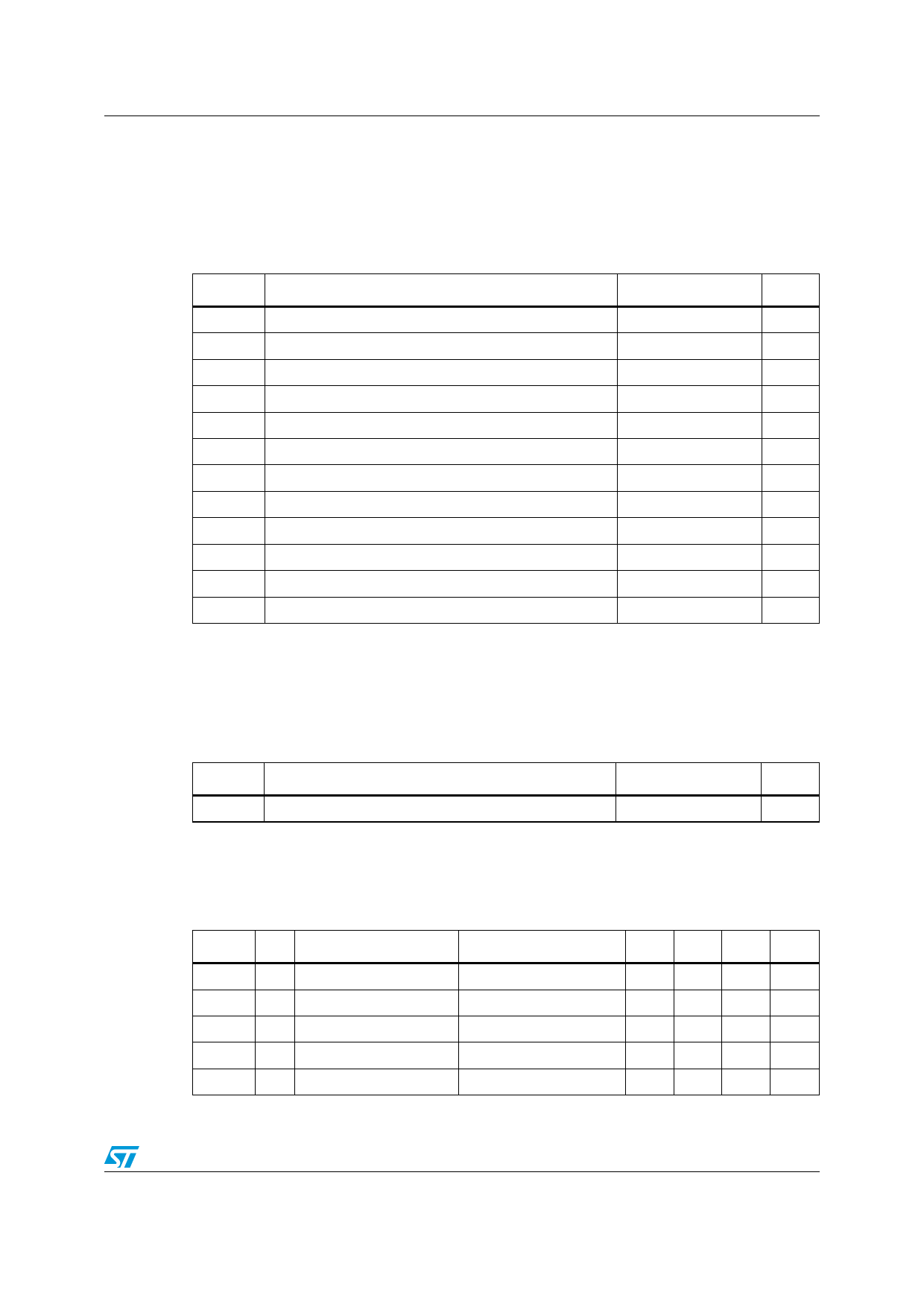
Absolute maximum ratings
Table 1. Absolute maximum ratings
Symbol
Parameter
Value
Unit
Vout
Vcc
Vboot
Vhvg
Vlvg
Vi
Vdiag
Vcin
dVout/dt
Ptot
Tj
Tstg
Output voltage
Supply voltage
Floating supply voltage
High-side gate output voltage
Low-side gate output voltage
Logic input voltage
Open drain forced voltage
Comparator input voltage
Allowed output slew rate
Total power dissipation (TJ = 85 °C)
Junction temperature
Storage temperature
-3 to Vboot - 18
- 0.3 to +18
-1 to 618
- 1 to Vboot
-0.3 to Vcc +0.3
-0.3 to Vcc +0.3
-0.3 to Vcc +0.3
-0.3 to 10 V
50
750
150
-50 to 150
V
V
V
V
V
V
V
V
V/ns
mW
°C
°C
ESD immunity for pins 12, 13 and 14 is guaranteed up to 900V (Human Body Model)
1.2
Thermal data
Table 2. Thermal data
Symbol
Parameter
Rth(JA) Thermal Resistance Junction to ambient
SO-14
165
Unit
°C/W
1.3
Recommended operating conditions
Table 3. Recommended operating conditions
Symbol Pin
Parameter
Test condition
Min Typ Max Unit
Vout 12 Output voltage
(1)
VBS (2) 14 Floating supply voltage
(1)
fsw
Switching frequency
HVG,LVG load CL = 1 nF
Vcc
4 Supply voltage
TJ
Junction temperature
-45
580 V
17
V
400 kHz
17
V
125 °C
1. If the condition Vboot - Vout < 18 V is guaranteed, Vout can range from -3 to 580 V
2. VBS = Vboot - Vout
3/17
Share Link: 