LS5260-0P データシートの表示(PDF) - Power-One Inc.
部品番号
コンポーネント説明
メーカー
LS5260-0P Datasheet PDF : 27 Pages
| |||
Cassette Style
100 Watt AC-DC Converters
S Series PFC
D Undervoltage Monitor
The input and/or output undervoltage monitoring circuit op-
erates independently of the built-in input undervoltage lock-
out circuit. A logic "low" (JFET output) or "high" signal (NPN
output) is generated at pin 20 as soon as one of the moni-
tored voltages drops below the preselected threshold level
Ut. The return for this signal is Vo1–. The D output recovers
when the monitored voltage(s) exceed(s) Ut + Uh. The
threshold level Uti is adjusted in the factory. The threshold
level Uto is either adjusted by a potentiometer, accessible
through a hole in the front cover, or factory adjusted to a
fixed value specified by the customer.
Option D exists in various versions D0...DD as shown in the
following table.
Table 18: Undervoltage monitoring functions
Output type
JFET
NPN
D1
D5
D2
D6
D3
D7
D4
D8
D0
D9
Monitoring
Ui
Uo1
no
yes
yes
no
yes
yes
no
yes
no
yes
yes
yes
Minimum adjustment range
of threshold level U t
U ti
Uto
-
3.5...40 V 1
355V DC 4
-
355V DC 4
(0.95...0.985 Uo1) 2
-
(0.95...0.985 Uo1) 2
-
3.5...40 V 3
355V DC 4
3.5...40 V 3
Typical hysteresis Uho [% of Ut]
for U t min...U t max
Uho
2.5...0.6
-
"0"
"0"
2.5...0.6
2.5...0.6
DD
yes
yes 355V DC 4
3.5...40 V 1
2.5...0.6
1 Threshold level adjustable by potentiometer
2 Fixed value. Tracking if Uo1 adjusted via R-input, option P or sense lines.
3 The threshold level permanently adjusted according to customer specification ±2% at 25°C. Any value within the specified range is
basically possible but causes a special type designation in addition to the standard option designations (D0/D9)!
4 Option D monitors the boost regulator output voltage. The trigger level is adjusted in the factory to 355 V DC.
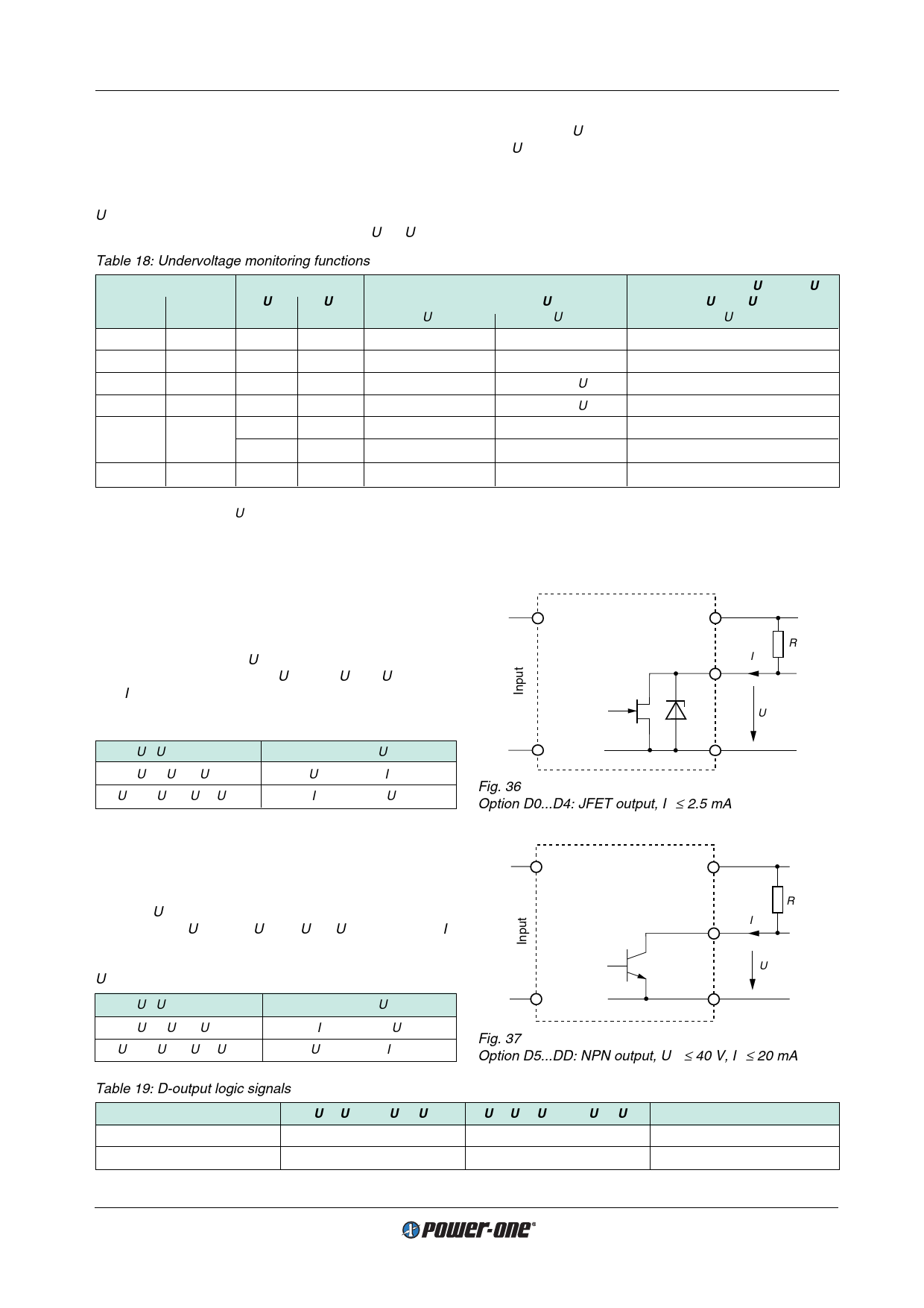
JFET output (D0…D4):
Connector pin D is internally connected via the drain-
source path of a JFET (self-conducting type) to the nega-
tive potential of output 1. UD ≤ 0.4 V (logic low) corresponds
to a monitored voltage level (Ui and/or Uo1) <Ut. The cur-
rent ID through the JFET should not exceed 2.5 mA. The
JFET is protected by a 0.5 W Zener diode of 8.2 V against
external overvoltages.
Ui, Uo1 status
Ui or Uo1 < Ut
Ui and Uo1 > Ut + Uh
D output, UD
low, L, UD ≤ 0.4 V at ID = 2.5 mA
high, H, ID ≤ 25 µA at UD = 5.25 V
11006
Vo1+
Rp
ID
D
UD
Vo1–
Fig. 36
Option D0...D4: JFET output, ID ≤ 2.5 mA
NPN output (D5...DD):
Connector pin D is internally connected via the collector-
emitter path of a NPN transistor to the negative potential of
output 1. UD < 0.4 V (logic low) corresponds to a monitored
voltage level (Ui and/or Uo1) > Ut + Uh. The current ID
through the open collector should not exceed 20 mA. The
NPN output is not protected against external overvoltages.
UD should not exceed 40 V.
Ui, Uo1 status
D output, UD
Ui or Uo1 < Ut
Ui and Uo1 > Ut + Uh
high, H, ID ≤ 25 µA at UD = 40 V
low, L, UD ≤ 0.4 V at ID = 20 mA
Table 19: D-output logic signals
Version of D
D1, D2, D3, D4, D0
D5, D6, D7, D8, D9, DD
Ui < Ut resp. Uo < Ut
low
high
11007
Vo1+
Rp
ID
D
UD
Vo1–
Fig. 37
Option D5...DD: NPN output, Uo1 ≤ 40 V, ID ≤ 20 mA
Ui > Ut + Uh resp. Uo > Ut
high
low
Configuration
JFET
NPN
Edition 01/01.2001
23/27
Share Link: 