MAX8515E_K データシートの表示(PDF) - Maxim Integrated
部品番号
コンポーネント説明
メーカー
MAX8515E_K Datasheet PDF : 10 Pages
| |||
Wide-Input 0.6V Shunt Regulators for
Isolated DC-to-DC Converters
VIN
1.8V
R3
C1
0.1µF
IN
OUT
MAX8515A
MAX8515
PGND
GND
FB
VOUT
0.6V/20mA
R1 = SHORT
R2 = OPEN
C2
1.0µF
R1
VIN (V) R3 (Ω)
3.3 135
10 470
R2
28 1.33k
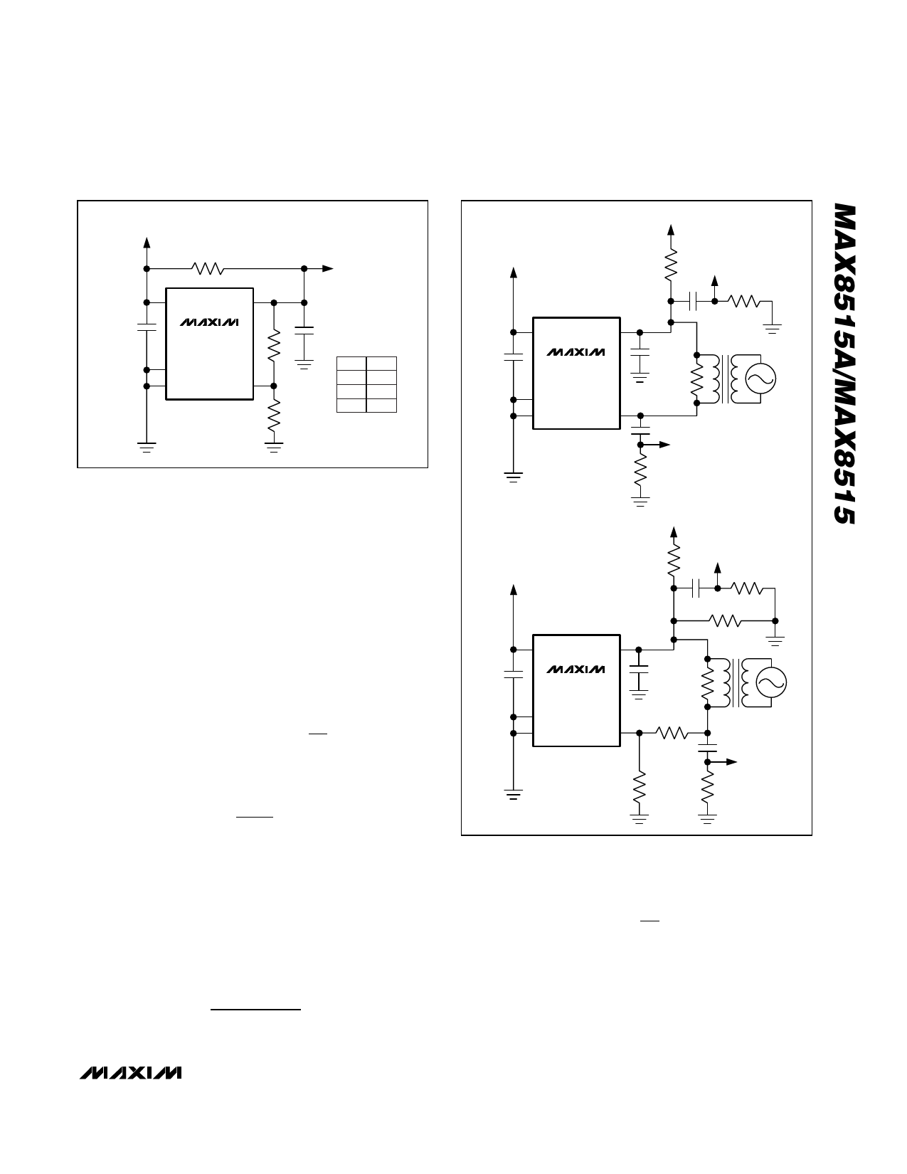
Figure 1. MAX8515A/MAX8515 Typical Application Circuit,
Shunt Regulator/Adjustable Voltage Reference
Optical Feedback
Setting VOUT
Figure 3 displays an application circuit using the
MAX8515A/MAX8515 in an opto-isolated feedback cir-
cuit. The maximum bias current for the photodiode is
set with R1. The isolated DC-to-DC converter compen-
sation circuit is formed with R2, C3, and C4. Resistors
R3 and R4 set the isolated DC-to-DC converter output
voltage. C1 decouples the input supply and C2 is
needed to stabilize the MAX8515A/MAX8515. Calculate
VREG with the following equation:
VREG = 0.6 ×
1 +
R3
R4
Set R4 to 10kΩ and calculate R3 by:
R3
=
VOUT
VFB
- 1
×
R4
For example, given a regulator output voltage of 1.8V
and R4 = 10kΩ, R3 is found to be 20kΩ.
Compensation Circuit
A typical compensation scheme is depicted in Figure 3.
C3 provides an integrator function that minimizes out-
put regulation error.
R2 provides additional phase compensation at the zero
frequency fz:
fZ
=
2π
×
1
R2
×
C3
5.6V
3.3V
VOUT = 0.6V
TEST CIRCUIT
0.1µF
IN
OUT
MAX8515A
MAX8515
PGND
GND
FB
GAIN = TEST/REFERENCE
1kΩ
TEST
2.2nF
1MΩ
0.82µF
50kΩ
2.2nF
REFERENCE
1MΩ
NETWORK
ANALYZER
SOURCE
11V
3.3V
VOUT = 6V
TEST CIRCUIT
115kΩ
1%
TEST
2.2nF
1MΩ
160kΩ
0.1µF
IN
OUT
MAX8515A
MAX8515
PGND
GND
FB
10kΩ
1%
GAIN = TEST/REFERENCE
0.1µF
50kΩ
90.1kΩ
1%
2.2nF
NETWORK
ANALYZER
SOURCE
REFERENCE
1MΩ
Figure 2. Test Circuits for Gain and Phase Plots
The midband gain is given by:
A = R2
R3
Add C4 for high-frequency noise rejection. Determine
R2 based on the midband gain required by the isolated
power supply. Choose fz based on the power supply
small-signal transfer function. Calculate C3 once fz
is known.
_______________________________________________________________________________________ 5
Share Link: 