MB91316 データシートの表示(PDF) - Fujitsu
部品番号
コンポーネント説明
メーカー
MB91316 Datasheet PDF : 71 Pages
| |||
MB91319R Series
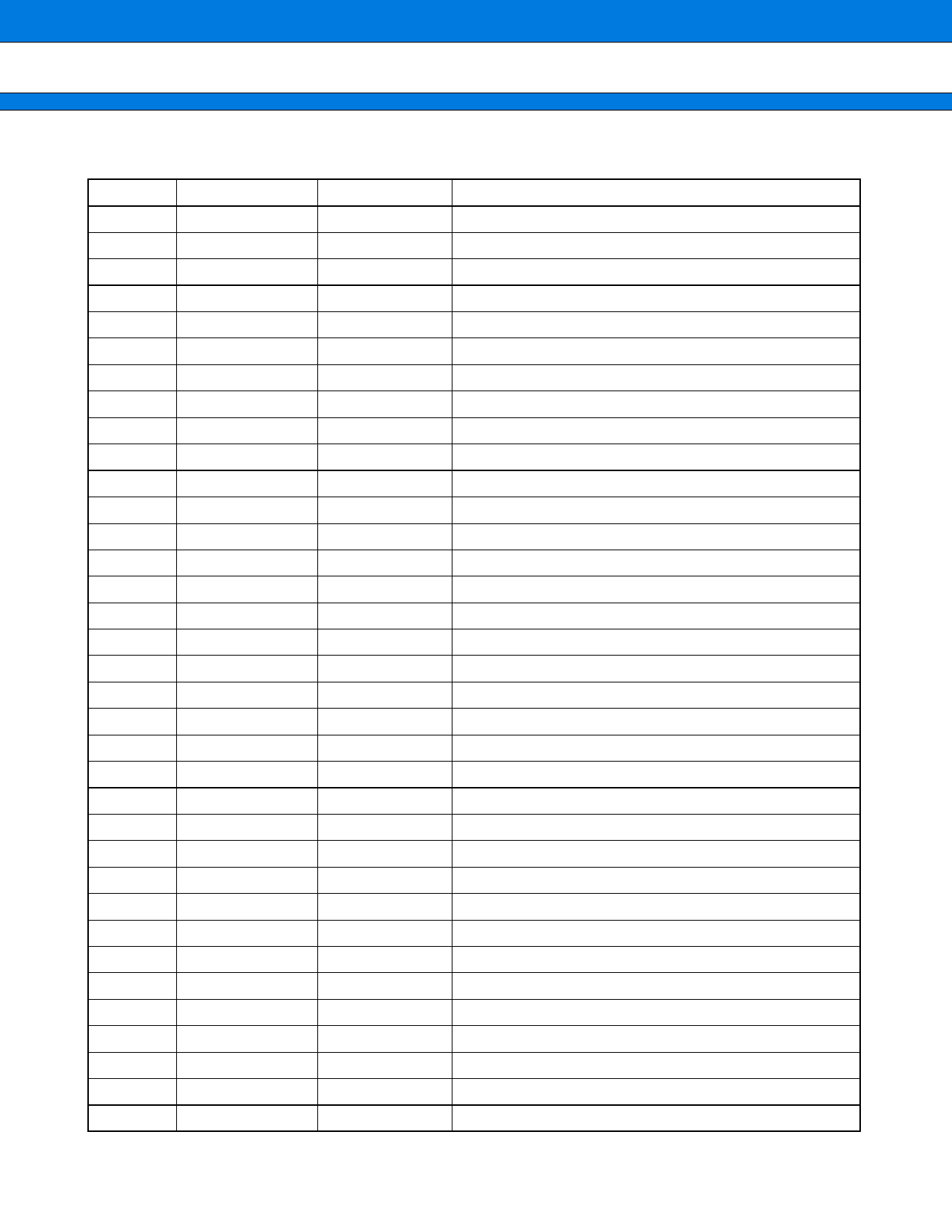
■ PIN DESCRIPTION
Pin No.
1
2
3
4
5
6
7
8
9
10
11
12
13
14
15
16
17
18
19
20
21
22
23
24
25
26
27
28
29
30
31
32
33
34
35
Pin Name
HSYNC1
HSYNC2
HSYNC3
VDDE
VSS
VGS1/VCI1
CPO1
VSSP1
VDDP1
VGS2/VCI2
CPO2
VSSP2
VDDP2
VGS3/VCI3
CPO3
VSSP3
VDDP3
VDDR
VREF
VR0
ROUT
VSSR
VDDG
GOUT
VSSG
VDDB
BOUT
VSSB
VIN0
VIN1
VDDIS
VSSS
VDDI
AVCC
AVRH
I/O Circuit type*
Function
G
Vertical synchronous input 1
G
Vertical synchronous input 2
G
Vertical synchronous input 3
⎯
I/O power supply
⎯
Ground
⎯
Guard band ground
K
Charge pump output
⎯
Dot clock PLL ground
⎯
Dot clock PLL power supply
⎯
Guard band ground
K
Charge pump output
⎯
Dot clock PLL ground
⎯
Dot clock PLL power supply
⎯
Guard band ground
K
Charge pump output
⎯
Dot clock PLL ground
⎯
Dot clock PLL power supply
⎯
D/A power supply for R
K
Power supply reference input
K
Resistor connection pin
K
R output (analog)
⎯
D/A ground for R
⎯
D/A power supply for G
K
G output (analog)
⎯
D/A ground for G
⎯
D/A power supply for B
K
B output (analog)
⎯
D/A ground for B
K
Data slicer input 0
K
Data slicer input 1
⎯
Data slicer power supply
⎯
Data slicer ground
⎯
Internal logic power supply
⎯
A/D power supply
⎯
A/D reference power supply
6
(Continued)
Share Link: 