MGA-71543 データシートの表示(PDF) - HP => Agilent Technologies
部品番号
コンポーネント説明
メーカー
MGA-71543 Datasheet PDF : 24 Pages
| |||
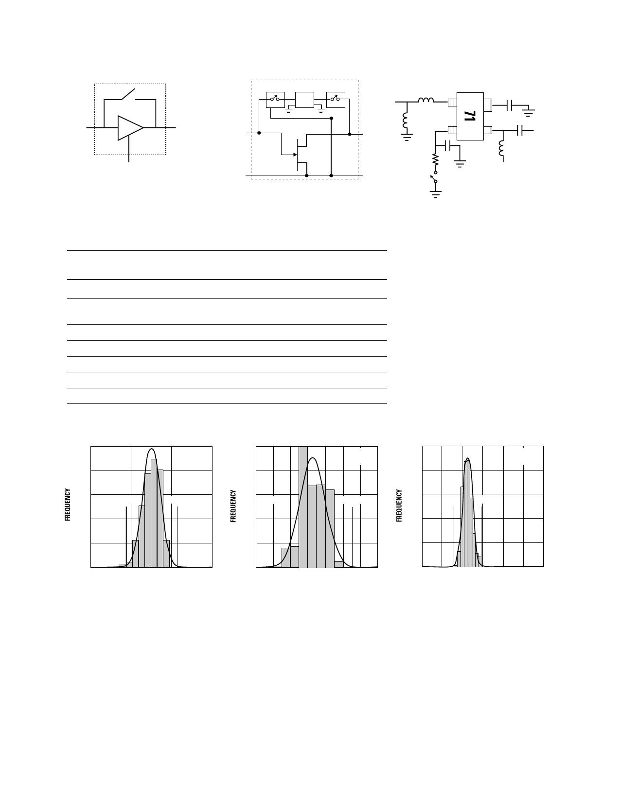
Functional Block Diagram
RF IN
RF OUT
Switch & Bias
Simplified Schematic
Input
& Vref
RF Gnd
++
––
Control
Gain FET
Evaluation Test Circuit
(single positive bias)
Input 1.5 nH
Output
& Vd
2.7 nH
Rbias
Vd
RF Gnd
& Vs
control
Output
MGA-71543 Absolute Maximum Ratings[1]
Symbol Parameter
Vd
Maximum Input to Output Voltage[4]
Vc
Maximum Input to Ground DC Voltage[4]
Id
Supply Current
Pd
Power Dissipation[2]
Pin
CW RF Input Power
Tj
Junction Temperature
TSTG
Storage Temperature
Units Absolute
Maximum
V
5.5
V
+.3
-5.5
mA
60
mW 240
dBm +15
°C
170
°C
-65 to +150
Operation
Maximum
4.2
+.1
-4.2
50
200
+10
150
-40 to +85
Thermal Resistance:[2,3]
θjc = 240°C/W
Notes:
1. Operation of this device in excess of any of
these limits may cause permanent damage.
2. Ground lead temperature at 25°C.
3. Thermal resistance measured by 150°C
Liquid Crystal Measurement method.
4. Maximum rating assumes other parameters
are at DC quiescent conditions.
Product Consistency Distribution Charts [5,6]
150
150
Cpk = 2.00
Std = 0.24
120
120
Cpk = 1.16
Std = 0.96
90
-3 Std
60
+3 Std
90
-3 Std
60
+3 Std
30
30
0
14.4
15.4
16.4
17.4
GAIN (dB)
Figure 1. Gain @ 2 GHz, 3V, 10 mA.
LSL = 14.4, Nominal = 15.9, USL = 17.4
Notes:
5. Distribution data sample size is 450 samples
taken from 9 different wafers. Future wafers
allocated to this product may have nominal
values anywhere within the upper and lower
specification limits.
6. Measurements made on production test
board, Figure 4. This circuit represents a
trade-off between an optimal noise match
and a realizable match based on production
test requirements at 10 mA bias current.
0
12
345 6
IIP3 (dBm)
78
Figure 2. IIP3 @ 2 GHz, 3V, 10 mA.
LSL = 1.0, Nominal = 3.0, USL = 8.0
Excess circuit losses have been de-
embedded from actual measurements.
Performance may be optimized for different
bias conditions and applications. Consult
Application Note for details.
150
Cpk = 2.33
Std = 0.02
120
90
-3 Std +3 Std
60
30
0
0.85 0.95
1.05 1.15 1.25
NF (dB)
1.35 1.45
Figure 3. NF @ 2 GHz, 3V, 10 mA.
LSL = 0.85, Nominal = 1.08, USL = 1.45
2
Share Link: 