MICRF218AYQS(2007) гГЗгГЉгВњгВЈгГЉгГИгБЃи°®з§ЇпЉИPDFпЉЙ - Micrel
йГ®еУБзХ™еПЈ
гВ≥гГ≥гГЭгГЉгГНгГ≥гГИи™ђжШО
гГ°гГЉгВЂгГЉ
MICRF218AYQS Datasheet PDF : 24 Pages
| |||
Micrel
Application Example
ANT
PCB Pattern
C2
1.5pF 50V
L1
39nH
C1
L2
6.8pF 68nH
+3V
C3
0.1µF 16V
MICRF218
Y1
9.8131MHz
U1 MICRF218AYQS
1 RO1
RO2 16
2 GNDRF
NC 15
3 ANT
RSSI 14
4 GNDRF
CAGC 13
5 VDD
CTH 12
6 IF_BW
SEL1 11
7 SEL0
DO 10
8 SHDN
GND 9
RSSI
DO
C4
0.1µF
16V
C5
4.7µF
6.3V
IF_BW CONTROL
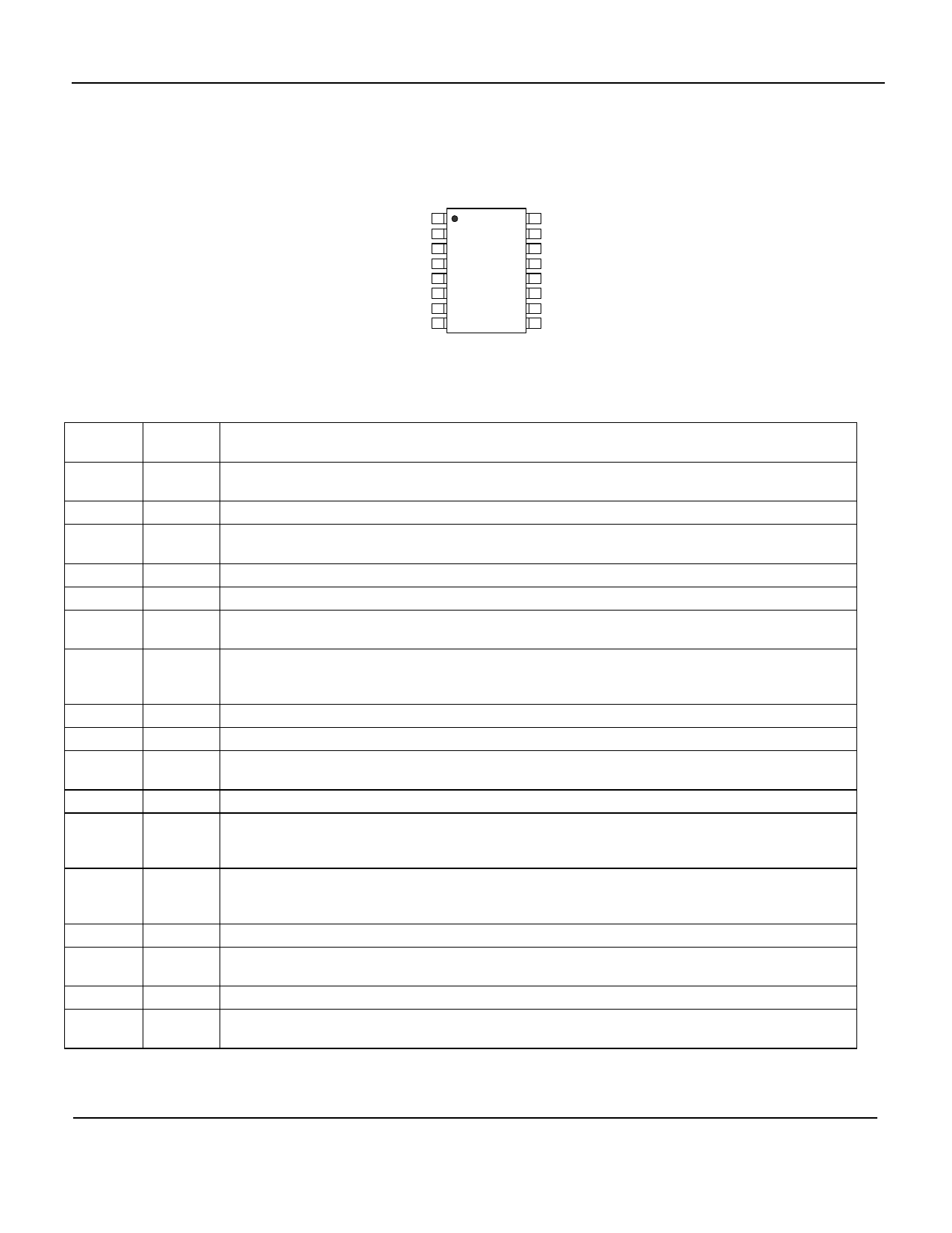
Pin Configuration
315MHz/315.802, 900Hz Baud Rate Example
RO1 1
GNDRF 2
ANT 3
GNDRF 4
Vdd 5
IF_BW 6
SEL0 7
SHDN 8
16 RO2
15 NC
14 RSSI
13 CAGC
12 CTH
11 SEL1
10 DO
9 GND
MICRF218AYQS
Pin Description
16-Pin
QSOP
1
2
3
4
5
6
7
8
9
Pin
Name
RO1
GNDRF
ANT
GNDRF
VDD
IF_BW
SEL0
SHDN
GND
Pin Function
Reference resonator input connection to Colpitts oscillator stage. May also be driven by external
reference signal of 1.5V p-p amplitude maximum.
Negative supply connection associated with ANT RF input.
RF signal input from antenna. Internally AC-Coupled. It is recommended that a matching network
with an inductor to RF ground is used to improve ESD protection.
Negative supply connection associated with ANT RF input.
Positive supply connection for all chip functions.
IF bandwidth control logic input. Use VDD for Wide IF Bandwidth or VSS for Narrow IF Bandwidth.
This pin must not be left floating, must be tied to VDD or VSS.
Logic control input with active internal pull-up. Used in conjunction with SEL1 to control the
demodulator low pass filter bandwidth. (See filter table for SEL0 and SEL1 in application
subsection)
Shutdown logic control input. Active internal pull-up and must be pulled low for Normal Operation.
Negative supply connection for all chip functions except RF input.
September 2007
2
M9999-090607
(408) 944-0800
Share Link: 