NCP1652A データシートの表示(PDF) - ON Semiconductor
部品番号
コンポーネント説明
メーカー
NCP1652A
ON Semiconductor
NCP1652A Datasheet PDF : 34 Pages
| |||
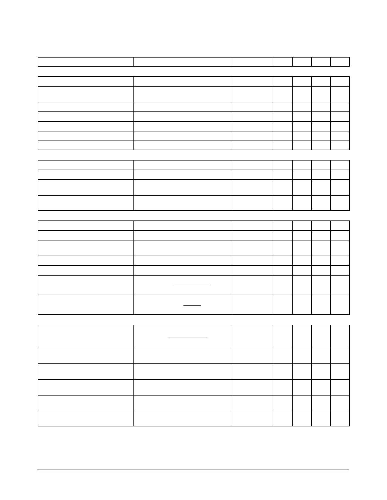
NCP1652, NCP1652A
ELECTRICAL CHARACTERISTICS (VCC = 15 V, VAC IN = 3.8 V, VFB = 2.0 V, VFF = 2.4 V, VLatch = open, VISPOS = −100 mV,
COUTA = 1 nF, CT = 470 pF, CIAVG = 0.27 nF, CLatch = 0.1 nF, CM = 10 nF, RIAVG = 76.8 kW, Rdelay = 49.9 kW,
COUTB = 330 pF, RRC = 43 kW, For typical Value TJ = 25°C, for min/max values TJ = −40°C to 125°C, unless otherwise noted)
Parameter
Test Condition
Symbol
Min Typ Max Unit
OSCILLATOR
Frequency
Frequency Modulation in Percentage
of fOSC
fosc
90 100 110 kHz
–
6.8
–
%
Frequency Modulation Period
–
6.8
–
ms
Ramp Peak Voltage
Ramp Valley Voltage
Maximum Duty Ratio
Ramp Compensation Peak Voltage
AC ERROR AMPLIFIER
Rdelay = open
VCT(peak)
VCT(valley)
D
–
4.0
–
V
–
0.10
–
V
94
−
–
%
VRCOMP(peak)
–
4
–
V
Input Offset Voltage (Note 3)
Error Amplifier Transconductance
Source Current
Sink Current
CURRENT AMPLIFIER
Ramp IAVG, VFB = 0 V
VAC COMP = 2.0 V, VAC IN = 2.0 V,
VFF = 1.0 V
VAC COMP = 2.0 V, VA C_IN = 2.0 V,
VFF = 5.0 V
ACVIO
gm
IEA(source)
IEA(sink)
40
–
mV
–
100
–
mS
25
70
–
mA
−25 −70
–
mA
Input Bias Current
Input Offset Voltage
Current Limit Threshold
VISPOS = 0 V
VAC COMP = 5.0 V, VISpos = 0 V
force OUTA high, VAC COMP = 3.0 V,
ramp VISPOS, VRamp_Comp = open
CAIbias
CAVIO
VILIM
40
53
80
mA
−20
0
20 mV
0.695 0.74 0.77 V
Leading Edge Blanking Duration
Bandwidth
tLEB
–
200
–
ns
–
1.5
– MHz
PWM Output Voltage Gain
Current Limit Voltage Gain (See
Current Sense Section)
REFERENCE GENERATOR
PWMk +
4
(VILIM * CAVIO)
V(AVG)
ISVK +
VISPOS
PWMk
ISVk
4.0 5.3 6.0 V/V
15.4 18.5 23 V/V
Reference Generator Gain
Reference Generator output voltage
(low input ac line and full load)
VAC_REF @ VFF 2
k+
VFB @ VAC_IN
VAC IN = 1.2 V, VFF = 0.765 V,
VFB = 4 V
k
–
0.55
–
V
RGout1
3.61 4.36 4.94 Vpk
Reference Generator output voltage
(high input ac line and full load)
Reference Generator output Voltage
(low input as line and minimum load)
Reference Generator output voltage
(high input ac line and minimum load)
VAC IN = 3.75 V, VFF = 2.39 V,
VFB = 4.0 V
VAC IN = 1.2 V, VFF = 0.765 V,
VFB = 2.0 V
VAC IN = 3.75 V, VFF = 2.39 V,
VFB = 2.0 V
RGout2
RGout3
RGout4
1.16 1.35 1.61 Vpk
1.85 2.18 2.58 Vpk
0.55 0.65 0.78 Vpk
Reference Generator output offset
voltage
RGoffset
−100
–
100 mV
3. Guaranteed by Design
http://onsemi.com
7
Share Link: 