NCV7381(2012) гГЗгГЉгВњгВЈгГЉгГИгБЃи°®з§ЇпЉИPDFпЉЙ - ON Semiconductor
йГ®еУБзХ™еПЈ
гВ≥гГ≥гГЭгГЉгГНгГ≥гГИи™ђжШО
гГ°гГЉгВЂгГЉ
NCV7381 Datasheet PDF : 23 Pages
| |||
NCV7381
Operating Mode Changes Caused by Internal Flags
Changes of some internal flags described in Table 3 can
force an operating mode transition complementing or
overruling the operating mode control by the digital inputs
STBN and EN which is shown in Figure 3:
вАҐ Setting the VBAT or VIO underвИТvoltage flag causes a
transition to the Sleep mode
вАҐ Setting the VCC underвИТvoltage flag, while the bus driver
is not in Sleep, causes a transition to the Standby mode
вАҐ Reset of the UnderвИТvoltage flag (i.e. recovery from
underвИТvoltage) reвИТenables the control of the chip by
digital inputs STBN and EN.
вАҐ Setting of the Wake flag causes the reset of all
underвИТvoltage flags and the NCV7381 transitions to the
Standby mode. The reset of the underвИТvoltage flags
allows the external power supplies to stabilize properly
if, for example, they were previously switched off
during Sleep mode.
uBus
FlexRay Bus Driver
NCV7381 contains a fullyвИТfeatured FlexRay bus driver
compliant with Electrical Physical Layer Specification Rev.
3.0.1. The transmitter part translates logical signals on
digital inputs TxEN, BGE and TxD into appropriate bus
levels on pins BP and BM. A transmission cannot be started
with Data_1. In case the transmitter is enabled for longer
than dBDTxActiveMax, the TxEN Timeout flag is set and the
current transmission is disabled. The receiver part monitors
bus pins BP and BM and signals the detected levels on digital
outputs RxD and RxEN. The different bus levels are defined
in Figure 5. The function of the bus driver and the related
digital pins in different operating modes is detailed in
Table 4 and Table 5.
вАҐ The transmitter can only be enabled if the activation of
the transmitter is initiated in Normal mode.
вАҐ The receiver function is enabled by entering a
normalвИТpower mode.
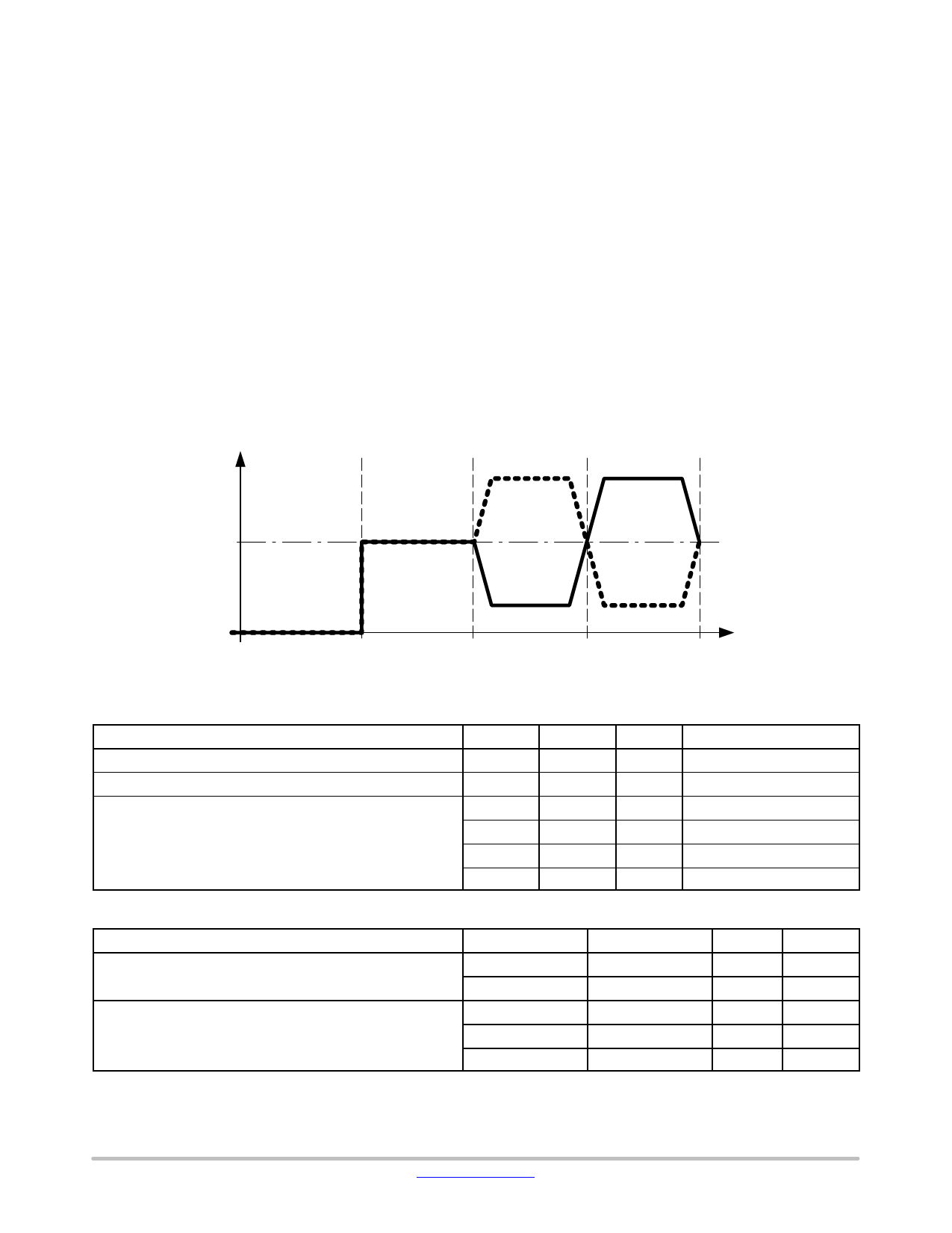
BP
VCC/2
Idle_LP
Idle
Data_0
Figure 5. FlexRay Bus Signals
BM
Data_1
Table 4. TRANSMITTER FUNCTION AND TRANSMITTERвИТRELATED PINS
Operating Mode
BGE
TxEN
Standby, GoвИТtoвИТsleep, Sleep
x
x
ReceiveвИТonly
x
x
Normal
0
x
1
1
1
0
1
0
TxD
Transmitted Bus Signal
x
Idle_LP
x
Idle
x
Idle
x
Idle
0
Data_0
1
Data_1
Table 5. RECEIVER FUNCTION AND RECEIVERвИТRELATED PINS
Operating Mode
Signal on Bus
Standby, GoвИТtoвИТsleep, Sleep
x
x
Normal,
ReceiveвИТonly
Idle
Data_0
Data_1
Wake flag
not set
set
x
x
x
RxD
High
Low
High
Low
High
RxEN
High
Low
High
Low
Low
http://onsemi.com
7
Share Link: 