AD8307ANZ1 データシートの表示(PDF) - Analog Devices
部品番号
コンポーネント説明
メーカー
AD8307ANZ1 Datasheet PDF : 25 Pages
| |||
Data Sheet
FEATURES
Complete multistage logarithmic amplifier
92 dB dynamic range: −75 dBm to +17 dBm to −90 dBm
using matching network
Single supply of 2.7 V minimum at 7.5 mA typical
DC to 500 MHz operation, ±1 dB linearity
Slope of 25 mV/dB, intercept of −84 dBm
Highly stable scaling over temperature
Fully differential dc-coupled signal path
100 ns power-up time, 150 μA sleep current
APPLICATIONS
Conversion of signal level to decibel form
Transmitter antenna power measurement
Receiver signal strength indication (RSSI)
Low cost radar and sonar signal processing
Network and spectrum analyzers (to 120 dB)
Signal level determination down to 20 Hz
True decibel ac mode for multimeters
GENERAL DESCRIPTION
The AD8307 is the first logarithmic amplifier made available in
an 8-lead SOIC_N package. It is a complete 500 MHz monolithic
demodulating logarithmic amplifier based on the progressive
compression (successive detection) technique, providing a
dynamic range of 92 dB to ±3 dB law conformance and 88 dB to
a tight ±1 dB error bound at all frequencies up to 100 MHz. The
AD8307 is extremely stable and easy to use, requiring no significant
external components. A single-supply voltage of 2.7 V to 5.5 V
at 7.5 mA is needed. A fast acting CMOS-compatible control
pin can disable the AD8307 to a standby current of 150 μA.
The AD8307 operates over the industrial temperature range of
−40°C to +85°C and is available in an 8-lead SOIC package and
an 8-lead PDIP.
Low Cost, DC to 500 MHz, 92 dB
Logarithmic Amplifier
AD8307
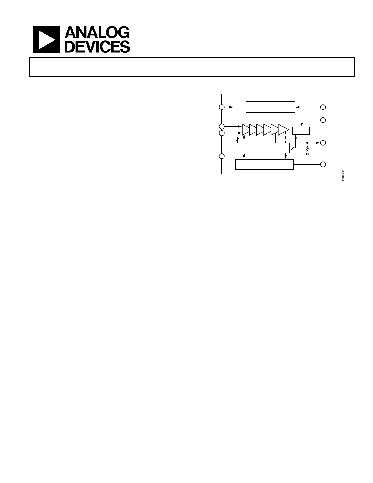
FUNCTIONAL BLOCK DIAGRAM
VPS 7
7.5mA
AD8307
BAND GAP REFERENCE
AND BIASING
6 ENB
INP
+INP
8
INM 1 1.1kΩ
–INP 3
SIX 14.3dB 900MHz
AMPLIFIER STAGES
COM 2
NINE DETECTOR CELLS
SPACED 14.3dB
INPUT-OFFSET
COMPENSATION LOOP
5 INT
MIRROR
2µA
/dB
2
4 OUT
12.5kΩ
COM
3 OFS
Figure 1.
Table 1. Next Generation Upgrades for the AD8307
Device No. Product Description
AD8310 15 ns Response Time, Buffered Output
ADL5513
Lower Input Range (80 dB), Operation to 4 GHz,
Higher Power Consumption
AD8309 Higher Input Range (100 dB), Limiter Output
Rev. E
Document Feedback
Information furnished by Analog Devices is believed to be accurate and reliable. However, no
responsibility is assumed by Analog Devices for its use, nor for any infringements of patents or other
rights of third parties that may result from its use. Specifications subject to change without notice. No
license is granted by implication or otherwise under any patent or patent rights of Analog Devices.
Trademarks and registered trademarks are the property of their respective owners.
One Technology Way, P.O. Box 9106, Norwood, MA 02062-9106, U.S.A.
Tel: 781.329.4700 ©1997–2015 Analog Devices, Inc. All rights reserved.
Technical Support
www.analog.com
Share Link: 