QL4016-3PLI データシートの表示(PDF) - Unspecified
部品番号
コンポーネント説明
メーカー
QL4016-3PLI
Unspecified
QL4016-3PLI Datasheet PDF : 18 Pages
| |||
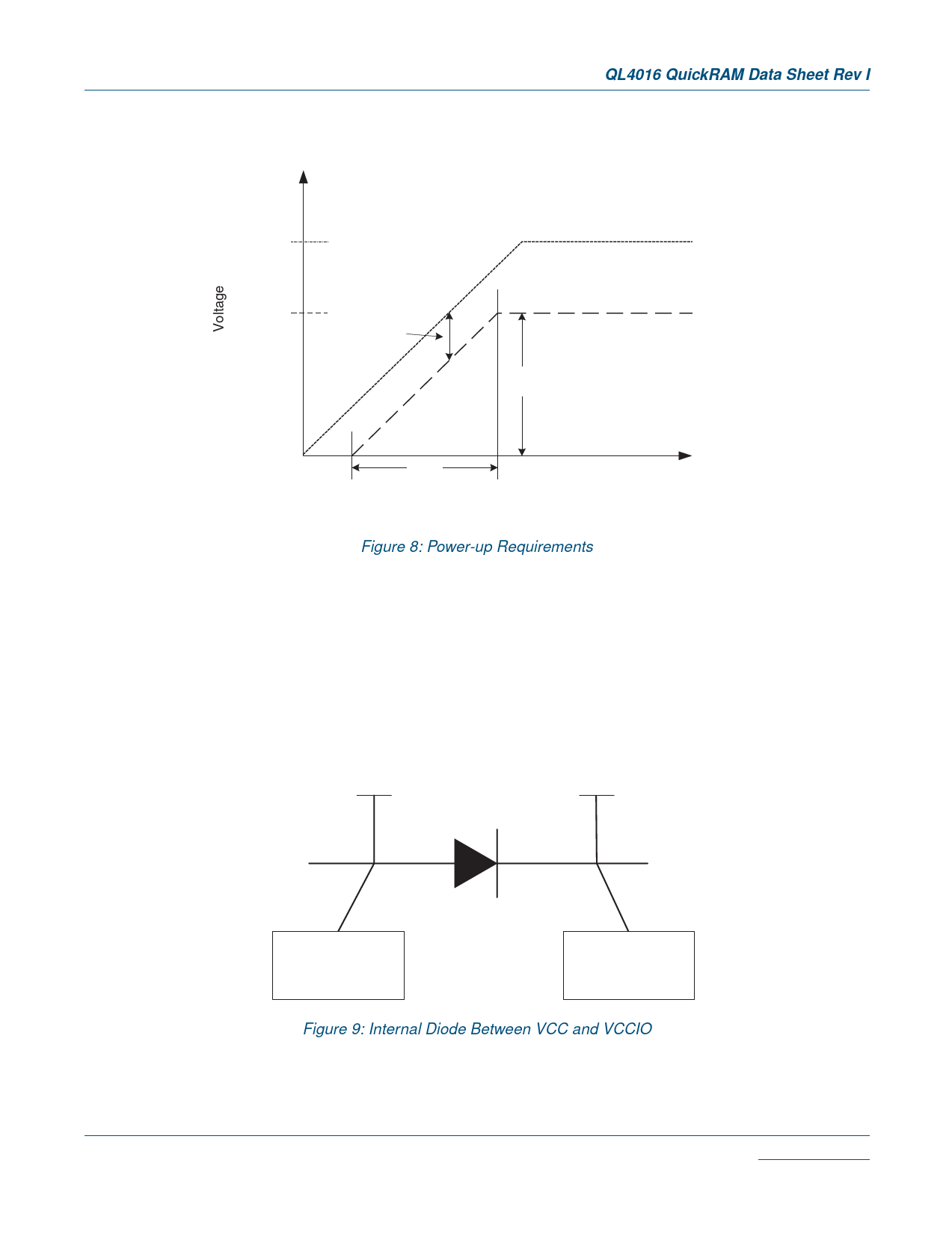
Power-up Sequencing
QL4016 QuickRAM Data Sheet Rev I
VCCIO
VCC
(VCCIO -VCC)MAX
VCC
400 us
Time
Figure 8: Power-up Requirements
The following requirements must be met when powering up the device (refer to Figure 8):
• When ramping up the power supplies keep (VCCIO -VCC)MAX ≤ 500 mV. Deviation from
this recommendation can cause permanent damage to the device.
• VCCIO must lead VCC when ramping the device.
• The power supply must take greater than or equal to 400 µs to reach VCC. Ramping
to VCC/VCCIO earlier than 400 µs can cause the device to behave improperly.
An internal diode is present in-between VCC and VCCIO, as shown in Figure 9.
V CC
V CCIO
Internal Logic
Cells, RAM
blocks, etc
IO Cells
Figure 9: Internal Diode Between VCC and VCCIO
© 2002 QuickLogic Corporation
•
www.quicklogic.com •• 11
•
•
•
Share Link: 