SL74HC257 データシートの表示(PDF) - System Logic Semiconductor
部品番号
コンポーネント説明
メーカー
SL74HC257 Datasheet PDF : 5 Pages
| |||
SL74HC257
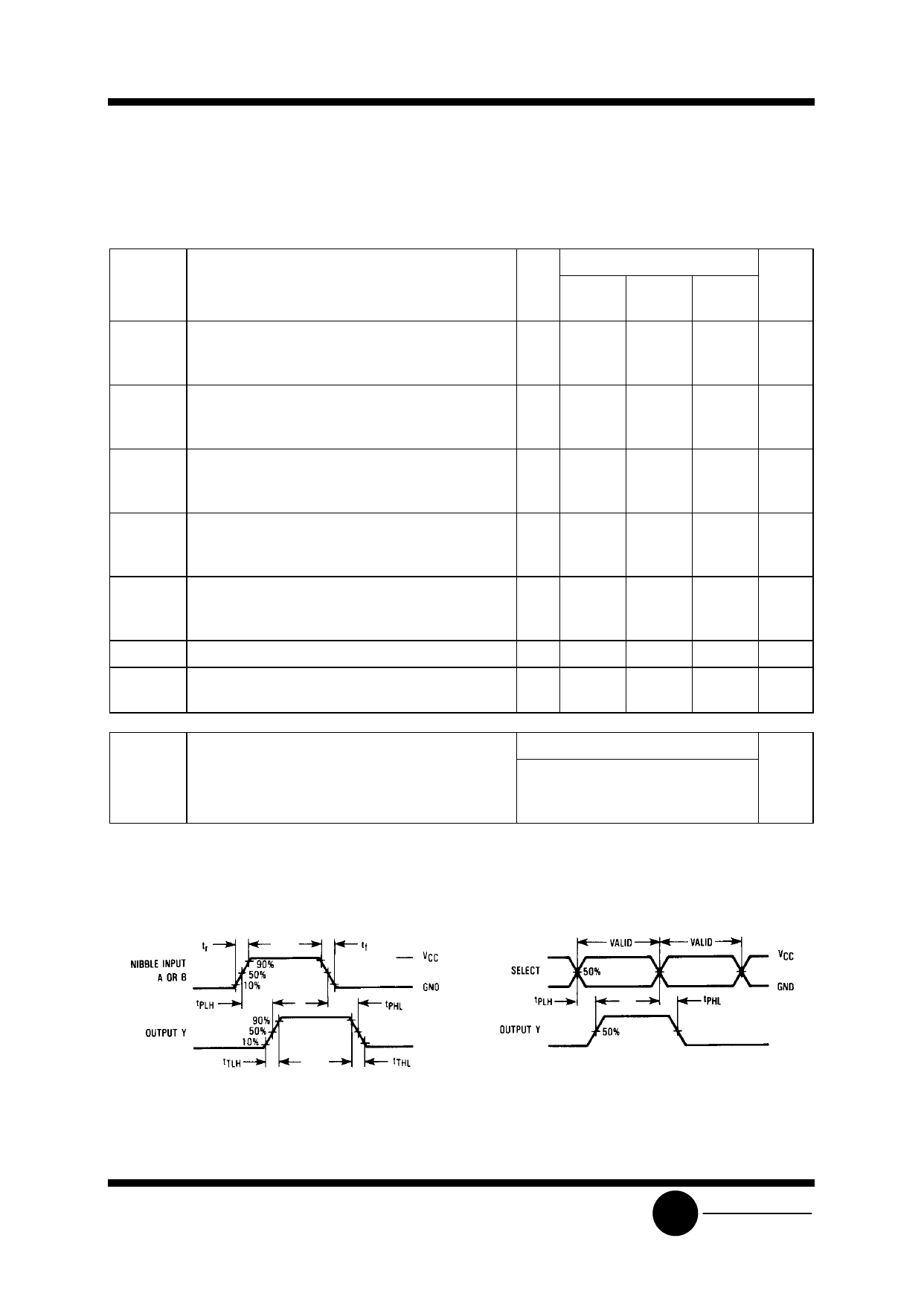
AC ELECTRICAL CHARACTERISTICS(CL=50pF,Input tr=tf=6.0 ns)
Symbol
Parameter
tPLH, tPHL Maximum Propagation Delay, Nibble A or B to
Output Y (Figures 1and 4)
tPLH, tPHL Maximum Propagation Delay , Select to
Output Y (Figures 2 and 4)
tPLZ, tPHZ Maximum Propagation Delay , Output Enable to
Output Y (Figures 3 and 5)
tPZL, tPZH Maximum Propagation Delay , Output Enable to
Output Y (Figures 3 and 5)
tTLH, tTHL Maximum Output Transition Time, Any Output
(Figures 1 and 4)
CIN
Maximum Input Capacitance
COUT Maximum Three-State Output Capacitance
(Output in High-Impedance State)
VCC
Guaranteed Limit
V 25 °C to ≤85°C ≤125°C Unit
-55°C
2.0 100
125
150
ns
4.5 20
25
30
6.0 17
21
26
2.0 100
125
150
ns
4.5 20
25
30
6.0 17
21
26
2.0 150
190
225
ns
4.5 30
38
45
6.0 26
33
38
2.0 150
190
225
ns
4.5 30
38
45
6.0 26
33
38
2.0 60
75
90
ns
4.5 12
15
18
6.0 10
13
15
-
10
10
10
pF
-
15
15
15
pF
Power Dissipation Capacitance (Per Package)
CPD Used to determine the no-load dynamic power
consumption:
PD=CPDVCC2f+ICCVCC
Typical @25°C,VCC=5.0 V
39
pF
Figure 1. Switching Waveforms
Figure 2. Switching Waveforms
SLS
System Logic
Semiconductor
Share Link: 