SX1781 データシートの表示(PDF) - Semtech Corporation
部品番号
コンポーネント説明
メーカー
SX1781 Datasheet PDF : 16 Pages
| |||
SX1781
PLL Frequency Synthesizer with integrated VCO
ADVANCED COMMUNICATIONS & SENSING
FINAL
DATASHEET
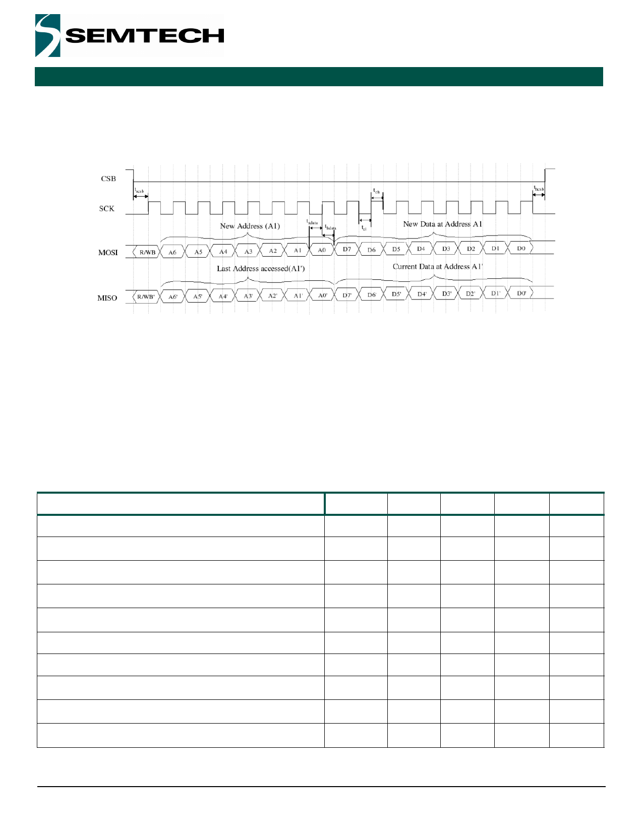
6.2. Write Register
To write a value into a configuration register the timing diagram below should be carefully followed by the uC.
Figure 2. SPI Write Timing
Note that when writing more than one registers successively, it is not compulsory to toggle CSB back high between two
cycles. The bytes are alternatively considered as address and value. In this instance, all new values will become effective
on the rising edge of CSB.
The Master latches the data on SCK falling edge and Slave samples the data on rising edge of SCK.
MISO pin reflects the previous Write access. For the Write access, MISO stays low. MISO pin is tri-stated when CSB is
high and when the device is in Sleep mode (SLEEPB is low).
Table 9 SPI Write Timings
Parameter
SPI Clock Frequency
Setup MOSI valid to SCKrising edge
Setup CSB falling edge to SCKrising edge
Delay SCKfalling edge to MISO valid
Delay CSBrising edge to MISO high-Z
SCK Low time
SCK High time
Hold MOSI valid after SCKrising edge
Hold CSB Low after SCKrising edge
Time between two accesses (CSBrising edge to CSBfalling edge)
Symbol
Fsck
tsdata
tscsb
td1
td2
tcl
tch
thdata
thcsb
tp
Minimum
-
4
Typical
-
-
Maximum
20
-
14
-
-
-
-
25
-
25
-
25
-
-
25
-
-
6
-
-
6
-
-
25
-
-
Unit
MHz
ns
ns
ns
ns
ns
ns
ns
ns
ns
Rev 1 - November 2008
©2008 Semtech Corp.
Page 8
www.semtech.com
Share Link: 