TS4601EIJT データシートの表示(PDF) - STMicroelectronics
部品番号
コンポーネント説明
メーカー
TS4601EIJT
STMicroelectronics
TS4601EIJT Datasheet PDF : 28 Pages
| |||
Electrical characteristics
3
Electrical characteristics
TS4601
3.1
Electrical characteristics tables
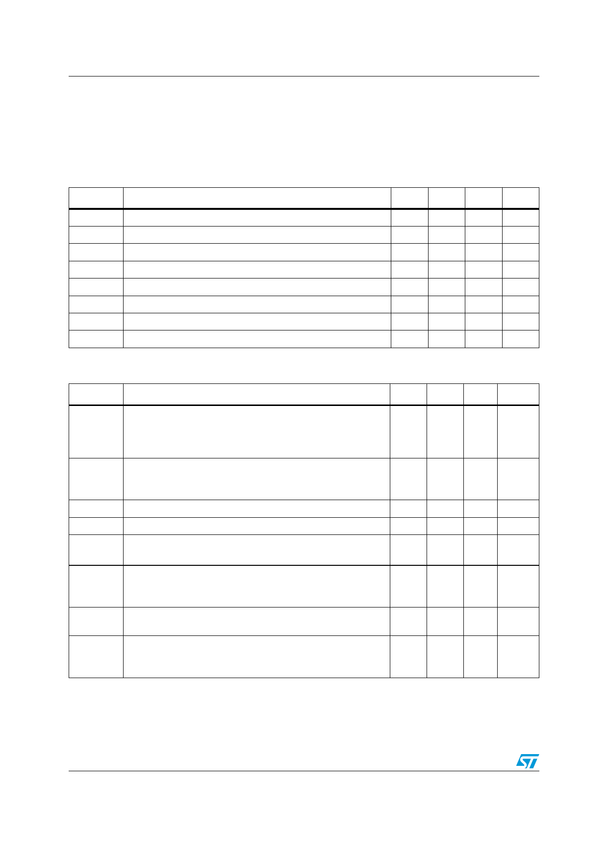
Table 5.
Symbol
Electrical characteristics of the I²C interface
from VCC=+2.9 V to VCC=+5.5 V, GND = 0 V, Tamb = 25° C (unless otherwise specified)
Parameter
Min. Typ. Max. Unit
VIL
VIH
VIL
VIH
FSCL
VOL
Iin
Low level input voltage on SDZ pins
High level input voltage on SDZ pins
Low level input voltage on SDA, SCL pins
High level input voltage on SDA, SCL pins
I2C clock frequency
Low level output voltage, SDA pin, Isink = 3mA
Input current on SDA, SCL from 0.4V to 4.5V
Pull-down resistor on SDZ
0.63
V
1.1
V
0.6
V
1.3
V
400 kHz
0.4
V
10
µA
480 600 720
kΩ
Table 6.
Symbol
Electrical characteristics of the amplifier
from VCC=+2.9 V to VCC=+5.5 V, GND = 0 V, Tamb = 25° C (unless otherwise specified)
Parameter
Min. Typ. Max. Unit
Quiescent supply current, no input signal, both channels
ICC
enabled, RL= 16Ω
VCC = 3.0V
VCC = 5.0V
ISTBY
Master standby current, No input signal
VSDZ= 0V
VSDZ= 0.35V, VCC= 5V
ISTBY
Vin
I²C standby current, no input signal
Input differential voltage range(1)
Output offset voltage
Voo
No input signal, RL = 32Ω
Maximum output voltage, in-phase signals
Vout
RL = 16Ω, THD+N = 1% max, f = 1kHz
RL = 10kΩ, Rs=15Ω, CL=1nF, THD+N = 1% max, f = 1kHz
Frequency RL = 16Ω, G = 0dB, Pout = 20mW, +/- 0.5dB (related to1kHz)
range Cin = 4.7µF
THD + N
Total harmonic distortion + noise, G = 0dB
RL = 16Ω, Po = 5mW, F = 1kHz
RL = 16Ω, Po = 10mW, 20Hz < F < 20kHz
mA
4.8
6
5.6
7
0.5
2
µA
10
75
µA
1.2
Vrms
-5
+5
mV
0.9
Vrms
1.6
10
22000 Hz
0.02
%
0.2
6/28
Share Link: 