UPD178P018A データシートの表示(PDF) - NEC => Renesas Technology
部品番号
コンポーネント説明
メーカー
UPD178P018A Datasheet PDF : 60 Pages
| |||
µPD178P018A
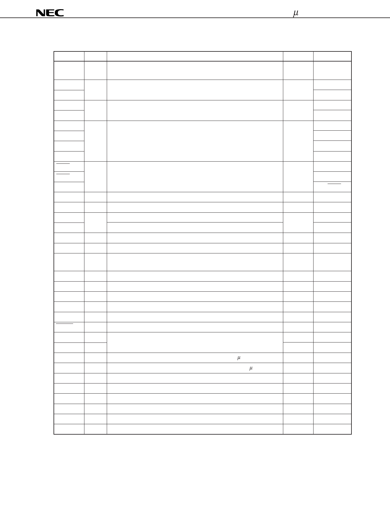
(2) Non-port pins (1 of 2)
Pin Name I/O
INTP0 to
INTP6
Input
SI0
Input
SI1
SO0
Output
SO1
SB0
I/O
SB1
SDA0
SDA1
SCK0
I/O
SCK1
SCL
STB
Output
BUSY
Input
TI1
Input
TI2
BEEP
Output
ANI0 to ANI5 Input
PWM0 to
PWM2
Output
EO0, EO1 Output
VCOL
Input
VCOH
Input
AMIFC
Input
FMIFC
Input
RESET
Input
X1
Input
X2
—
REGOSC
—
REGCPU
—
VDD
—
GND
—
VDDPORT
—
GNDPORT —
VDDPLL Note
—
GNDPLL Note —
Function
External maskable interrupt inputs with specifiable valid edges (rising
edge, falling edge, both rising and falling edges).
Serial interface serial data input
Serial interface serial data output
Serial interface serial data input/output
Serial interface serial clock input/output
Serial interface automatic transmit/receive strobe output
Serial interface automatic transmit busy input
External count clock input to 8-bit timer (TM1)
External count clock input to 8-bit timer (TM2)
Buzzer output
A/D converter analog input
PWM output
After Reset Alternate Function
Input
P00 to P06
Input
Input
Input
Input
Input
Input
Input
Input
Input
—
P25/SB0/SDA0
P20
P26/SB1/SDA1
P21
P25/SI0/SDA0
P26/SO0/SDA1
P25/SI0/SB0
P26/SO0/SB1
P27/SCL
P22
P27/SCK0
P23
P24
P33
P34
P36
P10 to P15
P132 to P134
Error out output from charge pump of the PLL frequency synthesizer
—
—
Inputs PLL local band oscillation frequency (In HF, MF mode).
—
—
Inputs PLL local band oscillation frequency (In VHF mode).
—
—
Inputs AM intermediate frequency counter.
—
—
Inputs FM intermediate frequency counter.
—
—
System reset input
—
—
Crystal resonator connection for system clock oscillation
—
—
—
—
Regulator for oscillator. Connected to GND via a 0.1-µF capacitor.
—
—
Regulator for CPU power supply. Connected to GND via a 0.1-µF capacitor.
—
—
Positive power supply
—
—
Ground
—
—
Positive power supply for port block
—
—
Ground for port block
—
—
Positive power supply for PLL
—
—
Ground for PLL
—
—
Note Connect a capacitor of approximately 1 000 pF between VDDPLL pin and GNDPLL pin.
11
Share Link: 