UPD75P3036GK データシートの表示(PDF) - NEC => Renesas Technology
部品番号
コンポーネント説明
メーカー
UPD75P3036GK Datasheet PDF : 64 Pages
| |||
µPD75P3036
3.1 Port Pins (2/2)
Pin name
P60
P61
P62
I/O
Alternate
function
I/O KR0
KR1
KR2
Function
This is a programmable 4-bit I/O port (PORT6).
Input and output can be specified in bit units.
Connection of an on-chip pull-up resistor can be
specified in 4-bit units by software.
8-bit
I/O
Yes
Status I/O circuit
after reset typeNote 1
Input
<F> -A
P63
KR3
P70
I/O KR4
P71
KR5
This is a 4-bit I/O port (PORT7).
Connection of an on-chip pull-up resistor can be
specified in 4-bit units by software.
Input
<F> -A
P72
KR6
P73
KR7
P80
I/O TI1
P81
TI2
This is a 4-bit I/O port (PORT8).
Connection of an on-chip pull-up resistor can be
specified in 4-bit units by software.
No
Input
<E> -E
P82
AN6
Y-B
P83
AN7
BP0
Output S24
BP1
S25
These pins are also used as 1-bit I/O port (BIT
PORT) segment output pin.
No
Note 2
H-A
BP2
S26
BP3
S27
BP4
Output S28
BP5
S29
BP6
S30
BP7
S31
Notes 1. Circuit types enclosed in brackets indicate Schmitt trigger input.
*
2. BP0 through BP7 select VLC1 as an input source.
However, the output levels change depending on the external circuit of BP0 through BP7 and VLC1.
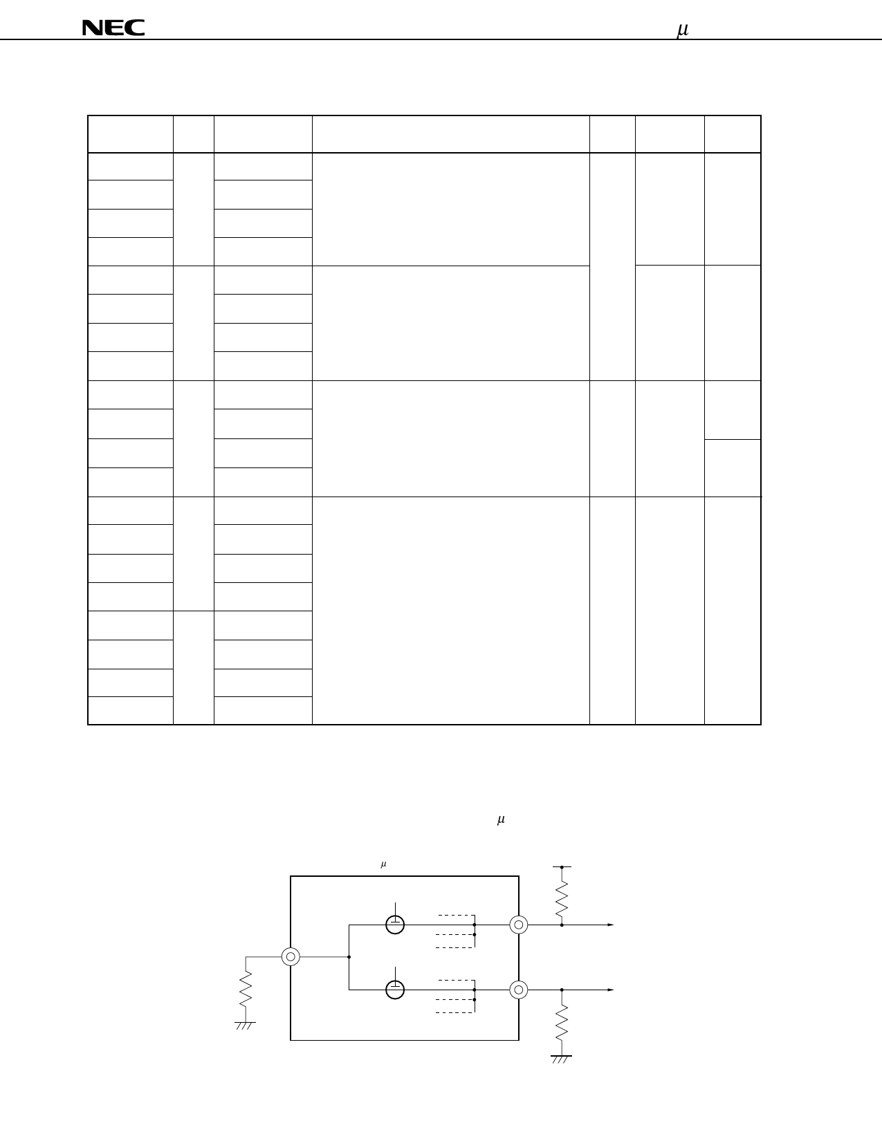
* Example Because BP0 through BP7 are mutually connected inside the µPD75P3036, the output levels of BP0 through
BP7 are determined by R1, R2, and R3.
µPD75P3036
VDD
ON
VLC1
R1
ON
R2
BP0
BP1
R3
8
Share Link: 