UPD75P3036GK データシートの表示(PDF) - NEC => Renesas Technology
部品番号
コンポーネント説明
メーカー
UPD75P3036GK Datasheet PDF : 64 Pages
| |||
µPD75P3036
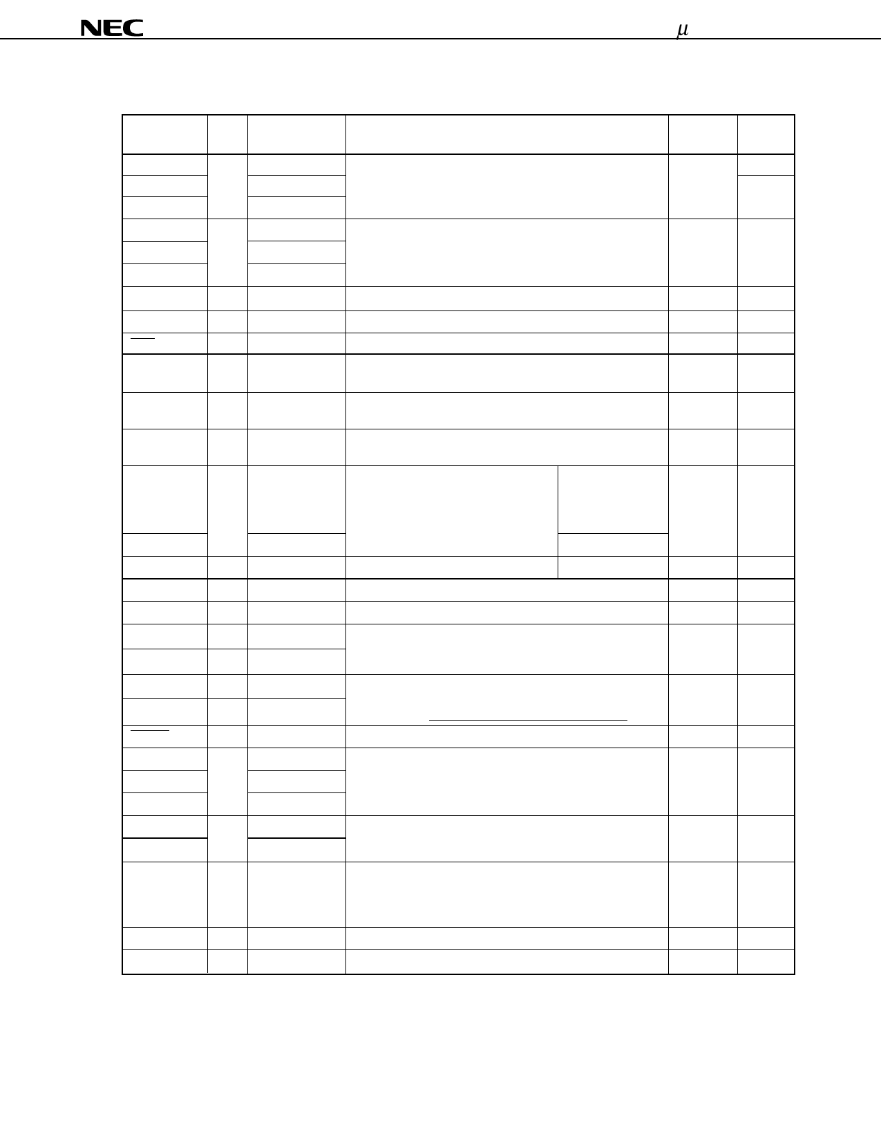
3.2 Non-port Pins (1/2)
Pin name
I/O
Alternate
function
Function
Status I/O circuit
after reset typeNote
TI0
Input P13
TI1
P80
External event pulse input to timer/event counter
Input
<B> -C
<E> -E
TI2
P81
PTO0
Output P20
Timer/event counter output
Input
E-B
PTO1
P21
PTO2
P22/PCL
PCL
Output P22/PTO2
Clock output
Input
E-B
BUZ
Output P23
Frequency output (for buzzer or system clock trimming)
Input
E-B
SCK
I/O P01
Serial clock I/O
Input
<F> -A
SO/SB0
I/O P02
Serial data output
Serial data bus I/O
Input
<F> -B
SI/SB1
I/O P03
Serial data input
Serial data bus I/O
Input
<M> -C
INT4
INT0
INT1
Input P00
Input P10
P11
Edge detection vectored interrupt input
(valid for detecting both rising and falling edges)
Edge detection vectored interrupt input
(detected edge is selectable)
INT0/P10 can select noise elimination
circuit.
Noise elimination
circuit
/asynchronous
is selectable
Asynchronous
Input
Input
<B>
<B> -C
INT2
KR0 to KR3
KR4 to KR7
Input
Input
Input
P12
P60 to P63
P70 to P73
Rising edge detection test input
Asynchonous
Parallel falling edge detection test input
Parallel falling edge detection test input
Input
Input
Input
<B> -C
<F> -A
<F> -A
X1
Input
—
Ceramic/crystal oscillation circuit connection for main system
—
—
clock. If using an external clock, input to X1 and input
X2
—
—
inverted phase to X2.
XT1
Input
—
Crystal oscillation circuit connection for subsystem clock.
—
—
If using an external clock, input to XT1 and input inverted
XT2
—
—
phase to XT2. XT1 can be used as a 1-bit (test) input.
RESET
Input
—
System reset input (low level active)
—
<B>
MD0
MD1
MD2, MD3
I/O P30/LCDCL
P31/SYNC
P32, P33
Mode selection for program memory (PROM) write/verify
Input
E-B
D0 to D3
D4 to D7
VPP
VDD
I/O P40 to P43
Data bus for program memory (PROM) write/verify
Input
M-E
P50 to P53
—
—
Programmable power supply voltage for program memory
—
—
(PROM) write/verify.
For normal operation, connect to VDD.
Apply +12.5 V for PROM write/verify.
—
—
Positive power supply
—
—
VSS
—
—
Ground
—
—
Note Circuit types enclosed in brackets indicate Schmitt trigger input.
9
Share Link: 