USB1T20 データシートの表示(PDF) - Fairchild Semiconductor
部品番号
コンポーネント説明
メーカー
USB1T20 Datasheet PDF : 9 Pages
| |||
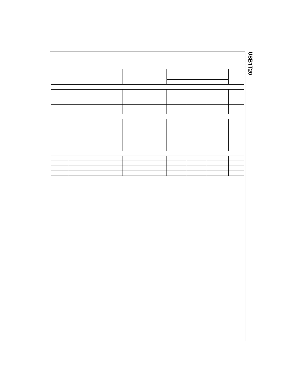
AC Electrical Characteristics (D+/D− Pins, Low Speed)
Over recommended range of supply voltage and operating free air temperature (unless otherwise noted).
VCC = 3.0V to 3.6V; CL = 200 pF to 600 pF; RL = 1.5kΩ on D− to VCC
Limits
Symbol
Parameter
Test Conditions
TAMB = −40°C to +85°C
Unit
Min
Typ
Max
Driver Characteristics
10% and 90%
tLR
Rise Time
tLF
Fall Time
tRFM
Rise/Fall Time Matching
VCRS
Output Signal Crossover Voltage
Driver Timings
Figure 1
Figure 1
(tR/tF)
75
300
ns
75
300
80
120
%
1.3
2.0
V
tPLH
Driver Propagation Delay
tPHL
(Vpo, Vmo/FSEO to D+/D−)
tPHZ
Driver Disable Delay
Figure 2
Figure 2
Figure 4
300
ns
300
ns
13
ns
tPLZ
(OE to D+/D−)
tPZH
Driver Enable Delay
Figure 4
Figure 4
13
ns
205
ns
tPZL
(OE to D+/D−)
Receiver Timings
Figure 4
205
ns
tPLH
Receiver Propagation Delay
tPHL
(D+, D− to RCV)
tPLH
Single-ended Receiver Delay
tPHL
(D+, D− to Vp, Vm)
Figure 3
Figure 3
Figure 3
Figure 3
18
ns
18
ns
28
ns
28
ns
5
www.fairchildsemi.com
Share Link: 