WM0831LID データシートの表示(PDF) - Wolfson Microelectronics plc
部品番号
コンポーネント説明
メーカー
WM0831LID
Wolfson Microelectronics plc
WM0831LID Datasheet PDF : 14 Pages
| |||
WM0831, WM0832
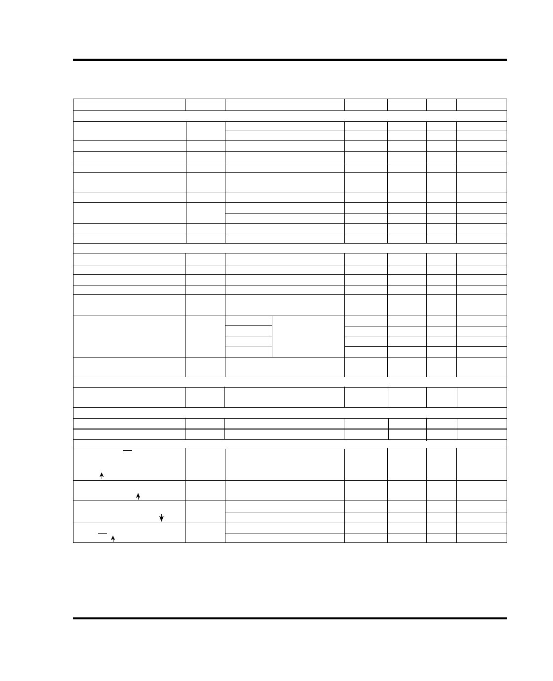
Electrical Characteristics (3.3V)
Vcc = 3.3V, fCLK = 250KHz, TA = TMIN to TMAX, tr = tf = 20 ns, unless otherwise stated.
PARAMETER
SYMBOL TEST CONDITIONS
MIN
Digital Inputs
High level output voltage
VOH
VCC = 3V, IOH = -360 µA
2.4
VCC = 3 V, IOH = -10 µA
2.8
Low level output voltage
VOL
VCC = 3V, IOH = 1.6 mA
High level input current
IIH
VIH = 3.6 V
Low level input current
IIL
VIL = 0 V
High level output (source)
IOH
VOH = 0 V, TA = 25oC
6.5
current
Low level output (sink) current IOL
VOL = 0V, TA = 25oC
8
High impedance-state
IOZ
VO = 3.3V, TA = 25oC
output current (DO)
VO = 0 V, TA = 25oC
Input capacitance
CI
Output capacitance
Co
Converter and Multiplexer
Total unadjusted error
TUE VREF = 3.3 V. (note 7)
Differential Linearity
(note 8)
8
Supply voltage variation error Vs(error) VCC = 3 V to 3.6 V
Common mode error
Differential mode
Common mode input voltage VICR (note 9)
GND-0.05
range
VCC+0.05
Standby input leakage
II(stdby) On-channel VI =3.3V at ON ch.
current (note 10)
Off-channel VI =0 V at OFF ch.
On-channel VI =0 V at ON ch.
Off-channel VI =3.3V at OFF ch.
Conversion time
tconv Excluding MUX addressing time
TYP
0.005
-0.005
15
16
0.01
-0.01
5
5
±1/16
±1/16
MAX
0.4
1
-1
3
-3
±1
±1/4
±1/4
1
-1
-1
1
8
Reference Inputs
Input resistance to
reference ladder
Total device
Supply current WM0831
Supply current WM0832
Timing Parameters
Setup time, CS low or
WM0832 data valid before
clock
Hold time, WM0832 data
valid after clock
Propagation delay time,
output data after clock
Output disable time, DO
after CS
Ri(REF) Can only be tested for WM0831 1.3
ICC
ICC
( note 11)
tsu
350
th
90
MSB data first. CL = 100 pF
tpd
LSB data first. CL = 100 pF
tdis
CL = 10 pF, RL = 10 kΩ
CL = 100 pF, RL = 2 kΩ
2.4
5.9
0.2 0.75
1.5
2.5
200
500
80
200
80
125
250
UNIT
V
V
V
µA
µA
mA
mA
µA
µA
pF
pF
LSB
Bits
LSB
LSB
V
µA
µA
µA
µA
clock
periods
kΩ
mA
mA
ns
ns
ns
ns
ns
ns
Wolfson Microelectronics
5
Share Link: 