ZXM64N02X(2004) データシートの表示(PDF) - Zetex => Diodes
部品番号
コンポーネント説明
メーカー
ZXM64N02X Datasheet PDF : 7 Pages
| |||
ZXM64N02X
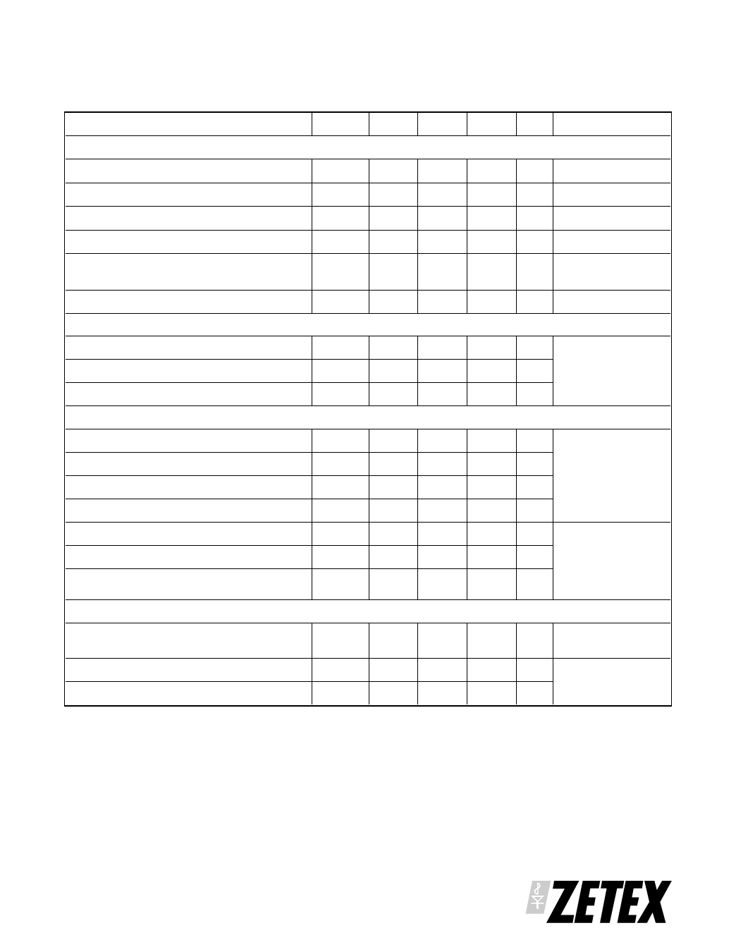
ELECTRICAL CHARACTERISTICS (at Tamb = 25°C unless otherwise stated).
PARAMETER
SYMBOL MIN. TYP. MAX. UNIT CONDITIONS.
STATIC
Drain-Source Breakdown Voltage
Zero Gate Voltage Drain Current
Gate-Body Leakage
Gate-Source Threshold Voltage
Static Drain-Source On-State Resistance
(1)
Forward Transconductance (3)
DYNAMIC (3)
V(BR)DSS 20
IDSS
IGSS
VGS(th) 0.7
RDS(on)
gfs
6.1
V
ID=250µA, VGS=0V
1
µA VDS=20V, VGS=0V
100
nA VGS=± 12V, VDS=0V
V
ID=250µA, VDS= VGS
0.040 Ω
0.050 Ω
VGS=4.5V, ID=3.8A
VGS=2.7V, ID=1.9A
S
VDS=10V,ID=1.9A
Input Capacitance
Output Capacitance
Reverse Transfer Capacitance
SWITCHING(2) (3)
Ciss
Coss
Crss
1100
350
100
pF
VDS=15 V, VGS=0V,
pF f=1MHz
pF
Turn-On Delay Time
Rise Time
Turn-Off Delay Time
Fall Time
Total Gate Charge
Gate-Source Charge
Gate Drain Charge
td(on)
tr
td(off)
tf
Qg
Qgs
Qgd
5.7
9.6
28.3
11.6
16
3.5
5.4
ns
ns VDD =10V, ID=3.8A
ns
RG=6.2Ω, RD=2.6Ω
(Refer to test
ns circuit)
nC
V D S= 16 V , V GS= 4 . 5V ,
nC ID=3.8A
(Refer to test
nC circuit)
SOURCE-DRAIN DIODE
Diode Forward Voltage (1)
VSD
0.95
Reverse Recovery Time (3)
trr
23.7
Reverse Recovery Charge(3)
Qrr
13.3
(1) Measured under pulsed conditions. Width=300µs. Duty cycle ≤2% .
(2) Switching characteristics are independent of operating junction temperature.
(3) For design aid only, not subject to production testing.
V
Tj=25°C, IS=3.8A,
V G S= 0V
ns Tj=25°C, IF=3.8A,
di/dt= 100A/µs
nC
ISSUE 1 - JUNE 2004
4
Share Link: 