NCP1247(2013) データシートの表示(PDF) - ON Semiconductor
部品番号
コンポーネント説明
メーカー
NCP1247 Datasheet PDF : 42 Pages
| |||
NCP1247
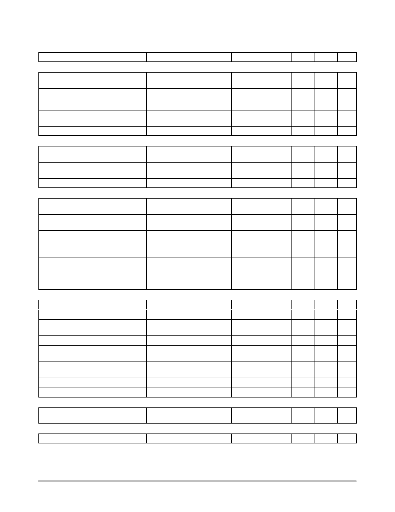
ELECTRICAL CHARACTERISTICS (For typical values TJ = 25°C, for min/max values TJ = −40°C to +125°C, VHV = 125 V,
VCC = 11 V unless otherwise noted)
Characteristics
Test Condition
Symbol
Min
Typ
Max
OSCILLATOR
Maximum on time
Maximum duty cycle (corresponding to
maximum on time at maximum switching
frequency)
fOSC = 65 kHz
fOSC = 100 kHz
fOSC = 65 kHz
fOSC = 100 kHz
tONmax(65kHz)
tONmax(100kHz)
DMAX
11.3
7.4
−
12.3
8.0
80
13.1
8.5
−
Frequency jittering amplitude, in percentage
of FOSC
Frequency jittering modulation frequency
FREQUENCY FOLDBACK
Ajitter
Fjitter
±4
±6
±8
85
125
165
Feedback voltage threshold below which
frequency foldback starts
VFB(foldS)
1.8
2.0
2.2
Feedback voltage threshold below which
frequency foldback is complete
VFB(foldE)
0.8
0.9
1.0
Minimum switching frequency
OUTPUT DRIVER
VFB = Vskip(in) + 0.1
fOSC(min)
23
27
32
Rise time, 10% to 90% of VCC
VCC = VCC(min) + 0.2 V,
CDRV = 1 nF
trise
−
40
70
Fall time, 90% to 10% of VCC
VCC = VCC(min) + 0.2 V,
CDRV = 1 nF
tfall
−
40
70
Current capability
VCC = VCC(min) + 0.2 V,
CDRV = 1 nF
DRV high, VDRV = 0 V
DRV low, VDRV = VCC
IDRV(source)
−
500
−
IDRV(sink)
−
800
−
Clamping voltage (maximum gate voltage)
VCC = VCCmax – 0.2 V, DRV high, VDRV(clamp)
11
13.5
16
RDRV = 33 kW, Cload = 220 pF
High−state voltage drop
VCC = VCC(min) + 0.2 V,
VDRV(drop)
−
−
1
RDRV = 33 kW, DRV high
CURRENT SENSE
Input Pull−up Current
Maximum internal current setpoint
Propagation delay from VIlimit detection to
DRV off
VCS = 0.7 V
VFB > 3.5 V
VCS = VILIM
Ibias
VILIM
tdelay
−
1
−
0.66 0.70 0.74
−
80
110
Leading Edge Blanking Duration for VILIM
Threshold for immediate fault protection
activation
tLEB
VCS(stop)
200
250
320
0.95 1.05 1.15
Leading Edge Blanking Duration for VCS(stop)
(Note 6)
tBCS
90
120
150
Soft−start duration
Frozen current setpoint
INTERNAL SLOPE COMPENSATION
From 1st pulse to VCS = VILIM
tSSTART
VI(freeze)
8
11
14
275
300
325
Slope of the compensation ramp
FEEDBACK
Scomp(65kHz)
−
−32.5
−
Scomp(100kHz)
−
−50
−
Internal pull−up resistor
TJ = 25°C
RFB(up)
15
20
25
5. Internal supply current only, currents sourced via FB pin is not included (current is flowing in GND pin only).
6. Guaranteed by design.
7. CS pin source current is a sum of Ibias and IOPC, thus at VHV = 125 V is observed the Ibias only, because IOPC is switched off.
Unit
ms
%
%
Hz
V
V
kHz
ns
ns
mA
V
V
mA
V
ns
ns
V
ns
ms
mV
mV /
ms
kW
http://onsemi.com
6
Share Link: 