1814 „Éá„Éľ„āŅ„ā∑„Éľ„Éą„ĀģŤ°®Á§ļÔľąPDFÔľČ - Linear Technology
ťÉ®ŚďĀÁē™ŚŹ∑
„ā≥„É≥„ÉĚ„Éľ„Éć„É≥„ÉąŤ™¨śėé
„É°„Éľ„āę„Éľ
1814 Datasheet PDF : 16 Pages
| |||
LT1813/LT1814
APPLICATIO S I FOR ATIO
Power dissipation is composed of two parts. The first is
due to the quiescent supply current and the second is due
to on-chip dissipation caused by the load current. The
worst-case load induced power occurs when the output
voltage is at 1/2 of either supply voltage (or the maximum
swing if less than 1/2 the supply voltage). Therefore PDMAX
is:
PDMAX = (V+ ‚Äď V‚Äď) ‚ÄĘ (ISMAX) + (V+/2)2/RL or
PDMAX = (V+ ‚Äď V‚Äď) ‚ÄĘ (ISMAX) + (V+ ‚Äď VOMAX) ‚ÄĘ (VOMAX/RL)
Example: LT1814S at 70¬įC, VS = ¬Ī5V, RL=100‚Ą¶
PDMAX = (10V) ‚ÄĘ (4.5mA) + (2.5V)2/100‚Ą¶ = 108mW
TJMAX = 70¬įC + (4 ‚ÄĘ 108mW) ‚ÄĘ (100¬įC/W) = 113¬įC
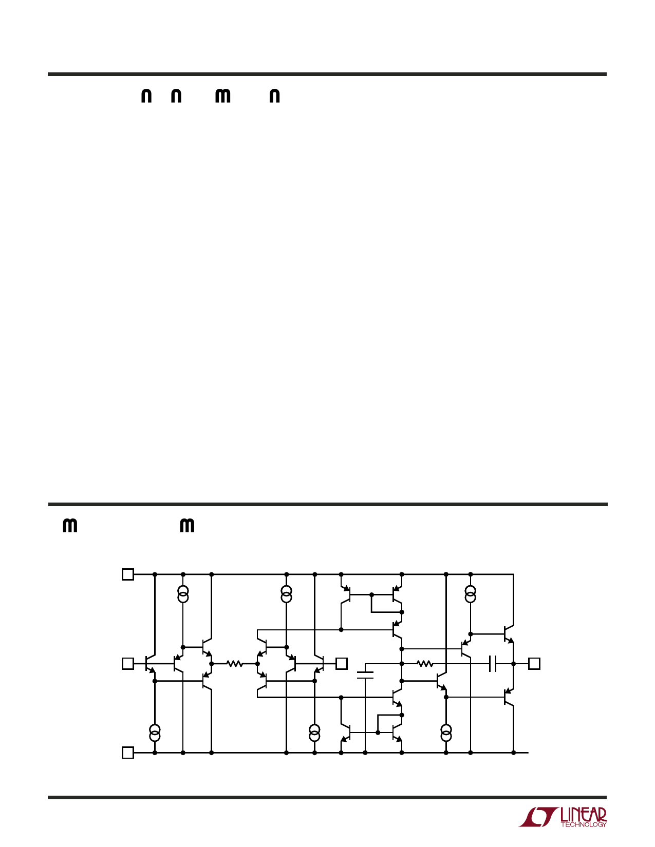
Circuit Operation
The LT1813/LT1814 circuit topology is a true voltage
feedback amplifier that has the slewing behavior of a
current feedback amplifier. The operation of the circuit can
be understood by referring to the Simplified Schematic.
Complementary NPN and PNP emitter followers buffer the
inputs and drive an internal resistor. The input voltage
appears across the resistor, generating current that is
mirrored into the high impedance node.
Complementary followers form an output stage that buff-
ers the gain node from the load. The input resistor, input
stage transconductance, and the capacitor on the high
impedance node determine the bandwidth. The slew rate
is determined by the current available to charge the gain
node capacitance. This current is the differential input
voltage divided by R1, so the slew rate is proportional to
the input step. Highest slew rates are therefore seen in the
lowest gain configurations.
The RC network across the output stage is bootstrapped
when the amplifier is driving a light or moderate load and
has no effect under normal operation. When a heavy load
(capacitive or resistive) is driven, the network is incom-
pletely bootstrapped and adds to the compensation at the
high impedance node. The added capacitance moves the
unity-gain frequency away from the pole formed by the
output impedance and the capacitive load. The zero cre-
ated by the RC combination adds phase to ensure that the
total phase lag does not exceed 180¬į (zero phase margin),
and the amplifier remains stable. In this way, the LT1813/
LT1814 are stable with up to 1000pF capacitive loads in
unity gain, and even higher capacitive loads in higher
closed-loop gain configurations.
W
W
SI PLIFIED SCHE ATIC (one amplifier)
V+
R1
+IN
CC
RC
‚ÄďIN
OUT
C
V‚Äď
12
1814 SS
18134fa
Share Link: 