M38748EAF-GP データシートの表示(PDF) - Mitsumi
部品番号
コンポーネント説明
メーカー
M38748EAF-GP Datasheet PDF : 92 Pages
| |||
MITSUBISHI MICROCOMPUTERS
3874 Group
SINGLE-CHIP 8-BIT CMOS MICROCOMPUTER
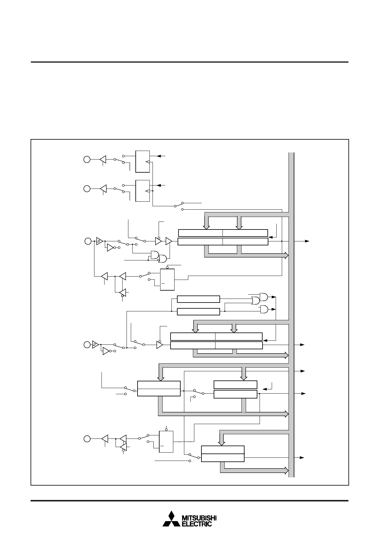
TIMERS
The 3874 group has five timers: timer X, timer Y, timer 1, timer 2,
and timer 3. Timer X and timer Y are 16-bit timers, and timer 1,
timer 2, and timer 3 are 8-bit timers.
All timers are down count timers. When the timer reaches “0016” or
“000016”, an underflow occurs at the next count pulse and the cor-
responding timer latch is reloaded into the timer and the count is
continued. When a timer underflows, the interrupt request bit cor-
responding to that timer is set to “1”.
Read and write operation on 16-bit timer must be performed for
both high and low-order bytes. When reading a 16-bit timer, read
the high-order byte first. When writing to a 16-bit timer, write the
low-order byte first. The 16-bit timer cannot perform the correct op-
eration when reading during the write operation, or when writing
during the read operation.
P56/RTP0
Real time port
control bit “1”
QD
P56 data for real time port
Data bus
P56 direction register “0” Latch
P56 latch
Real time port
control bit “1”
QD
P57/RTP1
P57 data for real time port
P57 direction register “0”
Latch
P57 latch
Real time port
control bit “0”
“1”
Timer X mode register
write signal
XIN/16
(XCIN/16 in φ = XCIN/2)
CNTR0 active Timer X operat-
edge switch bit
ing mode bit
“00”,“01”,“11”
Timer X stop
control bit
Timer X (low) latch (8)
Timer X write
control bit
Timer X (high) latch (8)
“0”
P54/CNTR0
Timer X (low) (8)
Timer X (high) (8)
“10”
“1”
Pulse width
measurement
mode CNTR0 active
edge switch bit “0” Q S
Pulse output mode
P54 direction register
“1”
P54 latch
T
Q
Pulse width HL continuously measurement mode
P55/CNTR1
Rising edge detection
Pulse output mode
XIN/16
(XCIN/16 in φ = XCIN/2)
Falling edge detection
Period
measurement mode
CNTR1 active
edge switch bit “00”,“01”,“11”
“0”
Timer Y stop
control bit
Timer Y (low) latch (8)
Timer Y (low) (8)
Timer Y (high) latch (8)
Timer Y (high) (8)
“1”
“10” Timer Y operating
mode bit
XIN/16
(XCIN/16 in φ = XCIN/2)
Timer 1 count source
selection bit
“0”
Timer 1 latch (8)
XCIN
“1”
Timer 1 (8)
Timer 2 count source
selection bit
“0”
Timer 2 latch (8)
Timer 2 (8)
“1”
XIN/16
(XCIN/16 in φ = XCIN/2)
Timer 2 write
control bit
Timer X
interrupt
Timer Y
interrupt
Timer 1
interrupt
Timer 2
interrupt
TOUT output
active edge
TOUT output
control bit
P50/TOUT
P50 direction register
switch bit “0”
“1”
P50 latch
QS
T
Q
“0”
Timer 3 latch (8)
TOUT output control bit
XIN/16(XCIN/16 in φ = XCIN/2)
Timer 3 (8)
“1”
Timer 3 count
source selection bit
Timer 3
interrupt
Fig. 22 Timer block diagram
30
Share Link: 