MC74VHCT14AD データシートの表示(PDF) - ON Semiconductor
部品番号
コンポーネント説明
メーカー
MC74VHCT14AD Datasheet PDF : 8 Pages
| |||
MC74VHCT14A
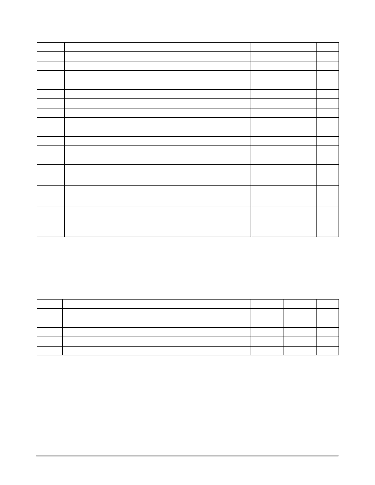
MAXIMUM RATINGS
Symbol
Parameter
Value
Unit
VCC
VIN
VOUT
VOUT
IIK
IOK
IO
ICC
IGND
TSTG
TL
TJ
qJA
DC Supply Voltage
DC Input Voltage
DC Output Voltage
Output in HIGH or LOW State (Note 1)
VCC = 0 V
DC Input Diode Current
DC Output Diode Current
DC Output Source/Sink Current
DC Supply Current per Supply Pin
DC Ground Current per Ground Pin
Storage Temperature Range
Lead Temperature, 1 mm from Case for 10 Seconds
Junction Temperature under Bias
Thermal Resistance
SOIC
TSSOP
*0.5 to )7.0
*0.5 to )7.0
*0.5 to VCC +0.5 V
*0.5 to 7.0
*20
$20
$25
$50
$50
*65 to )150
260
)150
125
170
V
V
V
V
mA
mA
mA
mA
mA
_C
_C
_C
_C/W
PD
Power Dissipation in Still Air
mW
SOIC
500
TSSOP
450
VESD
ESD Withstand Voltage
Human Body Model (Note 2)
> 2000
V
Machine Model (Note 3)
> 200
Charged Device Model (Note 4)
2000
ILatch–Up Latch–Up Performance
Above VCC and Below GND at 85_C (Note 5)
$300
mA
Maximum Ratings are those values beyond which damage to the device may occur. Exposure to these conditions or conditions beyond those
indicated may adversely affect device reliability. Functional operation under absolute maximum–rated conditions is not implied. Functional
operation should be restricted to the Recommended Operating Conditions.
1. IO absolute maximum rating must be observed.
2. Tested to EIA/JESD22–A114–A.
3. Tested to EIA/JESD22–A115–A.
4. Tested to JESD22–C101–A.
5. Tested to EIA/JESD78.
RECOMMENDED OPERATING CONDITIONS
Symbol
Parameter
VCC
Supply Voltage
VI
Input Voltage
VO
Output Voltage (Note 1)
VO
VCC = 0 V
TA
Operating Free–Air Temperature
Min
4.5
0
0
0
*55
Max
Unit
5.5
V
5.5
V
VCC
V
5.5
V
)125
_C
http://onsemi.com
2
Share Link: 