LT6658 データシートの表示(PDF) - Linear Technology
部品番号
コンポーネント説明
メーカー
LT6658 Datasheet PDF : 30 Pages
| |||
LT6658
Applications Information
Input Bypass Capacitance
Each input voltage pin requires a 0.1µF capacitor located
as close to the supply pin as possible. A 10µF capacitor
is recommended for each supply where the supply enters
the board. When the supply pins are connected together,
a single 0.1µF and single 10µF capacitor can be used.
The BYPASS pin requires a 1µF capacitor for stability.
Stability and Output Capacitance
The LT6658 is designed to be stable for any output ca-
pacitance between 1µF and 50µF, under any load condi-
tion, specified input voltage, or specified temperature.
Choosing a suitable capacitor is important in maintaining
stability. Preferably a low ESR and ESL capacitor should
be chosen. The value of the output capacitor will affect
the settling response.
Care should be exercised in choosing an output capacitor,
as some capacitors tend to deviate from their specified
value as operating conditions change.
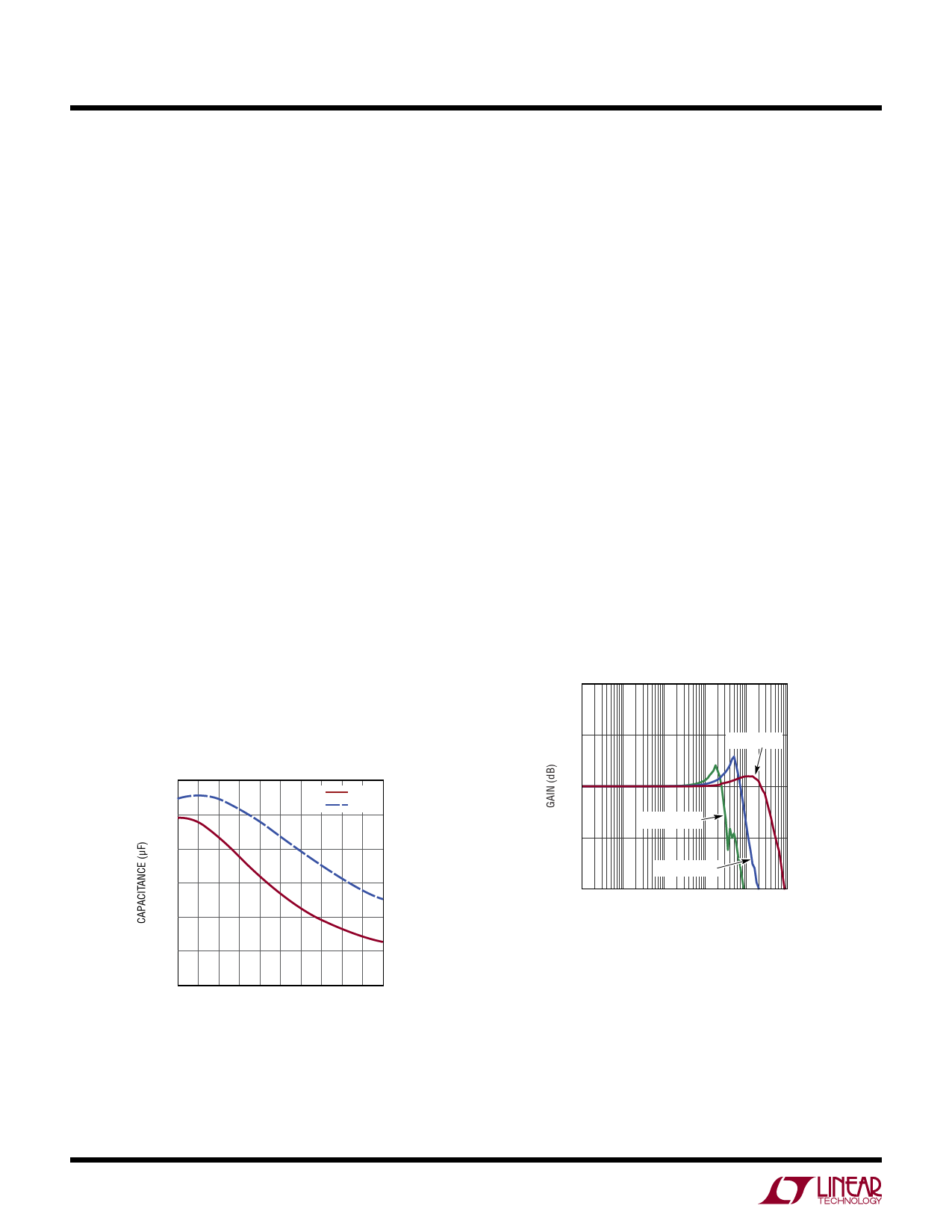
Although ceramic capacitors are small and inexpensive,
they can vary considerably over the DC bias voltage. For
example, the capacitance value of X5R and X7R capacitors
will change significantly over their rated voltage range as
shown in Figure 3. In this example the 1µF X5R capacitor
loses almost 75% of its value at its rated voltage of 10V.
X5R and X7R capacitors will also vary up to 20% or more
over a temperature range of –55°C to 125°C. This change
in capacitance will be combined with any DC bias voltage
variation.
Film capacitors do not vary much over temperature and
DC bias as much as X5R and X7R capacitors, but gener-
ally they are only rated to 105°C. Film capacitors are also
physically larger.
Effective series resistance (ESR) in the output capacitor
can add a zero to the loop response of the output buffers
creating an instability or excessive ringing. For the best
results keep the ESR at or below 0.2Ω.
One measure of stability is the closed loop response of
the output buffer. By driving the NR pin, a closed loop
response can be obtained. In Figure 4 the closed loop
response of the output buffer with three different output
capacitance values is shown. In the Figure 5 the same plot
is repeated with a 150mA load.
A large value electrolytic capacitor with a 1µF to 50µF ce-
ramic capacitor in parallel can be used on the output pins.
The buffers will be stable, and the bandwidth will be lower.
20
10
COUT1 = 1µF
1.2
X5R
X7R
1.0
0.8
0.6
0.4
0.2
0.0
0 1 2 3 4 5 6 7 8 9 10
DC BIAS (V)
6658 F03
Figure 3. Capacitance Value of a 1µF X7R Over Its Full Rated Voltage
0
COUT1 = 50µF
–10
–20
0.01
COUT1 = 10µF
0.1
1
10
100
1k
FREQUENCY (kHz)
6658 F04
Figure 4. LT6658 Closed Loop Response of the
Channel 1 Output Buffer for 3 Values of Output
Capacitance and No Load
6658f
14
For more information www.linear.com/LT6658
Share Link: 