R3111N171C データシートの表示(PDF) - RICOH Co.,Ltd.
部品番号
コンポーネント説明
メーカー
R3111N171C Datasheet PDF : 44 Pages
| |||
R3111x
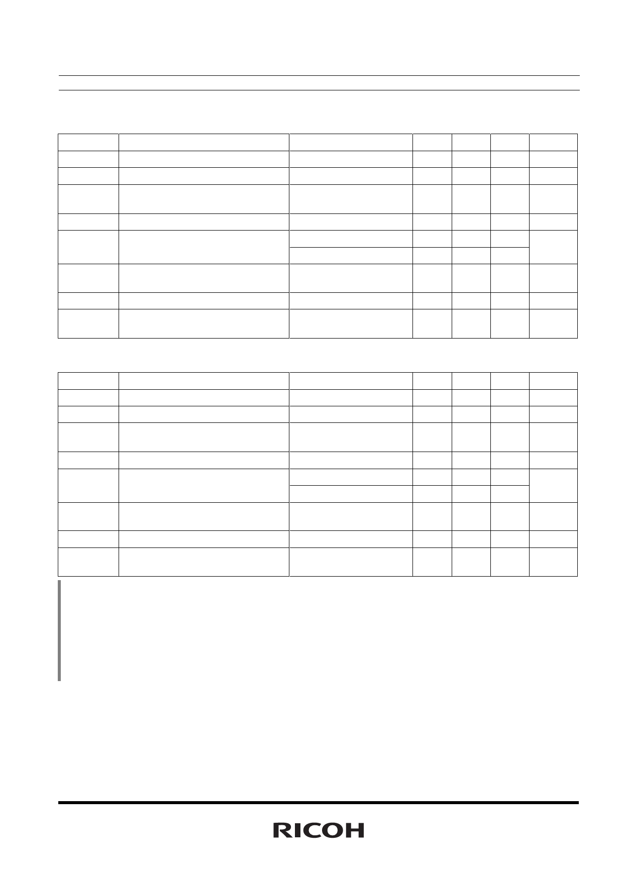
• R3111Q231B
Symbol
−VDET
VHYS
ISS
VDDH
VDDL
IOUT
tPLH
∆−VDET/
∆Topt
Item
Detector Threshold
Detector Threshold Hysteresis
Supply Current
Maximum Operating Voltage
Minimum Operating Voltage∗Note1
Output Current (Driver Output Pin)
Output Delay Time∗Note2
Detector Threshold Temperature
Coefficient
Conditions
VDD=2.2V
VDD=4.3V
Topt=25°C
−40°C <= Topt <= 85°C
Nch
VDS=0.50V,VDD=3.0V
−40°C <= Topt <= 85°C
Topt=25°C
Min. Typ. Max. Unit
2.254 2.300 2.346 V
0.069 0.115 0.161 V
0.9 2.7
1.1 3.3
µA
10
V
0.55 0.70
V
0.65 0.80
2.5
mA
100
µs
±100
ppm/°C
• R3111Q441B
Topt=25°C
Symbol
−VDET
VHYS
ISS
VDDH
VDDL
IOUT
tPLH
∆−VDET/
∆Topt
Item
Detector Threshold
Detector Threshold Hysteresis
Supply Current
Maximum Operating Voltage
Minimum Operating Voltage∗Note1
Output Current
(Driver Output Pin)
Output Delay Time∗Note2
Detector Threshold Temperature
Coefficient
Conditions
VDD=4.24V
VDD=6.4V
Topt=25°C
−40°C <= Topt <= 85°C
Nch
VDS=0.50V, VDD=5.5V
−40°C <= Topt <= 85°C
Min. Typ. Max. Unit
4.312 4.400 4.488 V
0.132 0.220 0.308 V
1.1 3.3
1.3 3.9
µA
10
V
0.55 0.70
V
0.65 0.80
2.5
mA
100
µs
±100
ppm/°C
∗Note1: Minimum operating voltage means the value of input voltage when output voltage maintains 0.1V or less. (In
the case of Nch Open Drain Output type, the output pin is pulled up with a resistance of 470kΩ to 5.0V.)
∗Note2: In the case of CMOS Output type: The time interval between the rising edge of VDD input pulse from 0.7V
to (+VDET)+2.0V and output voltage level becoming to ((+VDET)+2.0V)/2.
In the case of Nch Open Drain Output type: The output pin is pulled up with a resistance of 470kΩ to
5.0V, the time interval between the rising edge of VDD input pulse from 0.7V to (+VDET)+2.0V and output
voltage level becoming to 2.5V.
9
Share Link: 