MTP2N18 データシートの表示(PDF) - New Jersey Semiconductor
部品番号
コンポーネント説明
メーカー
MTP2N18 Datasheet PDF : 3 Pages
| |||
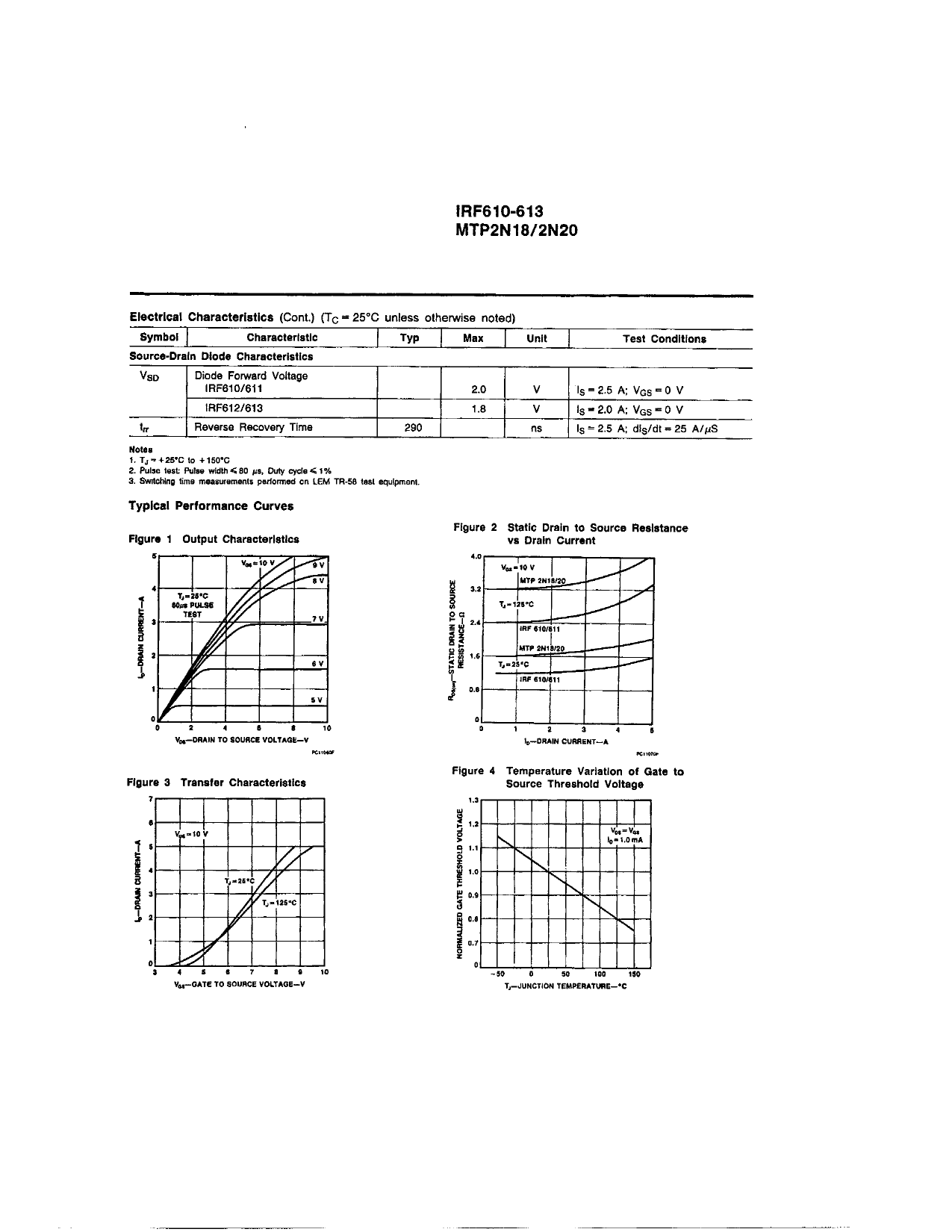
IRF610-613
MTP2N18/2N20
Electrical Characteristics (Cont.) (Tc - 25°C unless otherwise noted)
Symbol
Characteristic
Typ
Max
Unit
Source-Drain Diode Characteristics
VSD
Diode Forward Voltage
IRF610/611
2.0
V
IRF612/613
1.8
V
tir
Reverse Recovery Time
290
ns
Holes
1. Tj-+25'C to +150'C
2. Pulse test Pulse width < SO Its, Only cycle <1%
3. Switching time measurements performed en LEM TR-5B tast equipmGnl
Test Conditions
Is = 2.5 A; VGS = 0 V
ls - 2.0 A: VGS - 0 V
ls = 2.5 A; dls/dt = 25 A//jS
Typical Performance Curves
Figure 1 Output Characteristics
5
Figure 2 Static Drain to Source Resistance
vs Drain Current
0
1
4
6
I
10
Vj,—DRAIN TO SOURCE VOLTAQE-V
PCll44flf
Figure 3 Transfer Characteristics
7
<l
1*
V10
\-n>s
\
i*
i 4s <7 a«
vM-OATe TO SOURCE VOLTAOB-V
1
2
3
4
ID—DRAIN CURRENT—A
Figure 4 Temperature Variation of Gate to
Source Threshold Voltage
I0-1.0mA
I"
§ c'fl
1 0.7
z
0
Tj-JUNCTION TEMPERATURE—*C
Share Link: 