ADP2384 データシートの表示(PDF) - Analog Devices
部品番号
コンポーネント説明
メーカー
ADP2384 Datasheet PDF : 24 Pages
| |||
ADP2384
THEORY OF OPERATION
The ADP2384 is a synchronous step-down, dc-to-dc regulator
that uses a current mode architecture with an integrated high-
side power switch and a low-side synchronous rectifier. The
regulator targets high performance applications that require
high efficiency and design flexibility.
The ADP2384 operates from an input voltage that ranges from
4.5 V to 20 V and regulates the output voltage from 0.6 V to 90%
of the input voltage. Additional features that maximize design
flexibility include the following: programmable switching
frequency, programmable soft start, external compensation,
precision enable, and a power-good output.
CONTROL SCHEME
The ADP2384 uses a fixed frequency, peak current mode PWM
control architecture. At the start of each oscillator cycle, the
high-side N-MOSFET is turned on, putting a positive voltage
across the inductor. When the inductor current crosses the peak
inductor current threshold, the high-side N-MOSFET is turned
off and the low-side N-MOSFET is turned on. This puts a negative
voltage across the inductor, causing the inductor current to
decrease. The low-side N-MOSFET stays on for the rest of the
cycle (see Figure 17).
PRECISION ENABLE/SHUTDOWN
The EN input pin has a precision analog threshold of 1.17 V
(typical) with 100 mV of hysteresis. When the enable voltage
exceeds 1.17 V, the regulator turns on; when it falls below 1.07 V
(typical), the regulator turns off. To force the regulator to auto-
matically start when input power is applied, connect EN to PVIN.
The precision EN pin has an internal pull-down current source
(5 µA) that provides a default turn-off when the EN pin is open.
When the EN pin voltage exceeds 1.17 V (typical), the ADP2384
is enabled and the internal pull-down current source at the EN
pin decreases to 1 µA, which allows users to program the PVIN
UVLO and hysteresis.
INTERNAL REGULATOR (VREG)
The on-board regulator provides a stable supply for the internal
circuits. It is recommended that a 1 µF ceramic capacitor be placed
between the VREG pin and GND. The internal regulator includes
a current-limit circuit to protect the output if the maximum
external load current is exceeded.
Data Sheet
BOOTSTRAP CIRCUITRY
The ADP2384 includes a regulator to provide the gate drive
voltage for the high-side N-MOSFET. It uses differential sensing to
generate a 5 V bootstrap voltage between the BST and SW pins.
It is recommended that a 0.1 µF, X7R or X5R ceramic capacitor
be placed between the BST pin and the SW pin.
OSCILLATOR
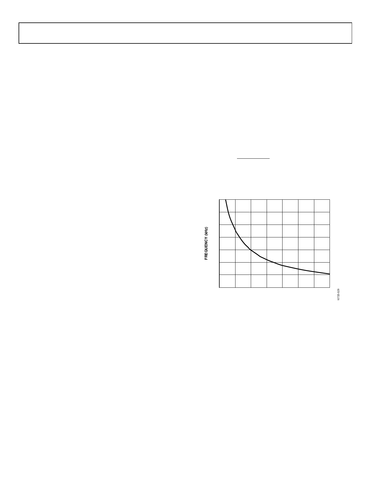
The ADP2384 switching frequency is controlled by the RT pin.
A resistor from RT to GND can program the switching frequency
according to the following equation:
fSW (kHz) = 69,120
RT (k Ω) + 15
A 100 kΩ resistor sets the frequency to 600 kHz, and a 42.2 kΩ
resistor sets the frequency to 1.2 MHz. Figure 29 shows the
typical relationship between fSW and RT.
1400
1200
1000
800
600
400
200
0
20
60
100
140
180
220
260
300
RT (kΩ)
Figure 29. Switching Frequency vs. RT
SYNCHRONIZATION
To synchronize the ADP2384, connect an external clock to the
SYNC pin. The frequency of the external clock can be in the range
of 200 kHz to 1.4 MHz. During synchronization, the regulator
operates in continuous conduction mode (CCM), and the rising
edge of the switching waveform runs 180° out of phase to the rising
edge of the external clock.
When the ADP2384 operates in synchronization mode,
a resistor must be connected from the RT pin to GND to
program the internal oscillator to run at 90% to 110% of the
external synchronization clock.
Rev. A | Page 12 of 24
Share Link: 