ML1350-5P データシートの表示(PDF) - LANSDALE Semiconductor Inc.
部品番号
コンポーネント説明
メーカー
ML1350-5P Datasheet PDF : 6 Pages
| |||
ML1350
LANSDALE Semiconductor, Inc.
ELECTRICAL CHARACTERISTICS (V+ = +12 Vdc, TA = +25°C, unless otherwise noted.)
Characteristics
Symbol
Min
Typ
Max
Unit
AGC Range, 45 MHz (5.0 V to 7.0 V) (Figure 1)
60
68
–
dB
Power Gain (Pin 5 grounded via a 5.1 kΩ resistor)
f = 58 MHz, BW = 4.5 MHz
See Figure 6(a)
f = 45 MHz, BW = 4.5 MHz
See Figure 6(a), (b)
f = 10.7 MHz, BW = 350 kHz
See Figure 7
f = 455 kHz, BW = 20 kHz
Ap
dB
–
48
–
46
50
–
–
58
–
–
62
–
Maximum Differential Voltage Swing
0 dB AGC
–30 dB AGC
VO
Vpp
–
20
–
–
8.0
–
Output Stage Current (Pins 1 and 8)
Total Supply Current (Pins 1, 2 and 8)
Power Dissipation
I1 + I8
–
IS
–
PD
–
5.6
–
mA
14
17
mAdc
168
204
mW
DESIGN PARAMETERS, Typical Values (V+ = +12 Vdc, TA = +25°C, unless otherwise noted.)
Frequency
Parameter
Symbol 455 kHz 10.7 MHz 45 MHz 58 MHz
Unit
Single–Ended Input Admittance
g11
0.31
0.36
0.39
0.5
mmho
b11
0.022
0.50
2.30
2.75
Input Admittance Variations with AGC
(0 dB to 60 dB)
Differential Output Admittance
∆g11
–
∆b11
–
–
60
–
µmho
–
0
–
g22
4.0
4.4
30
60
µmho
b22
3.0
110
390
510
Output Admittance Variations with AGC
(0 dB to 60 dB)
∆g22
–
∆b22
–
–
4.0
–
µmho
–
90
–
Reverse Transfer Admittance (Magnitude)
Forward Transfer Admittance
Magnitude
Angle (0 dB AGC)
Angle (–30 dB AGC)
Single–Ended Input Capacitance
Differential Output Capacitance
|y12|
|y21|
< y21
< y21
Cin
CO
< < 1.0 < < 1.0 < < 1.0 < < 1.0
µmho
160
160
–5.0
–20
–3.0
–18
7.2
7.2
1.2
1.2
200
180
mmho
–80
–105
Degrees
–69
–90
Degrees
7.4
7.6
pF
1.3
1.6
pF
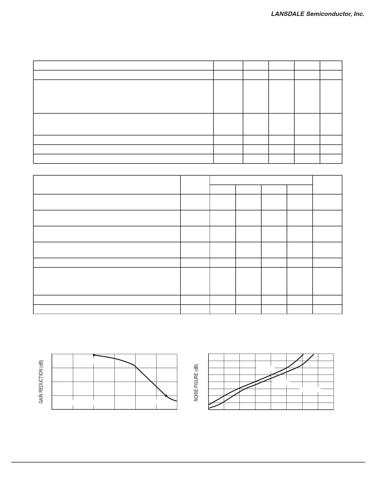
Figure 2. Typical Gain Reduction
0
IAGC = 0.1 mA
20
40
60
80
4.0
(Figures 6 and 7)
IAGC = 0.2 mA
5.0
6.0
7.0
VAGC, SUPPLY VOLTAGE (V)
Figure 3. Noise Figure versus Gain Reduction
22
20
18
58 MHz
16
14
45 MHz
12
(Figure 6)
10
8.0
6.0
0
10
20
30
40
GAIN REDUCTION (dB)
Page 2 of 6
www.lansdale.com
Issue A
Share Link: 