D2761EB データシートの表示(PDF) - Maxim Integrated
部品番号
コンポーネント説明
メーカー
D2761EB Datasheet PDF : 24 Pages
| |||
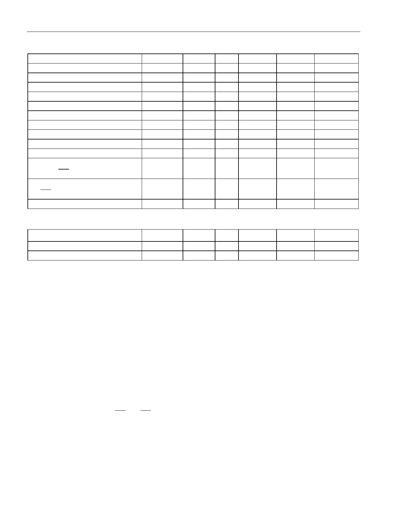
ELECTRICAL CHARACTERISTICS:
1-WIRE INTERFACE
PARAMETER
SYMBOL
Time Slot
Recovery Time
Write 0 Low Time
Write 1 Low Time
Read Data Valid
Reset Time High
Reset Time Low
Presence Detect High
Presence Detect Low
SWAP Timing Pulse Width
SWAP Timing Pulse Falling
tSLOT
tREC
tLOW0
tLOW1
tRDV
tRSTH
tRSTL
tPDH
tPDL
tSWL
tSWOFF
Edge to DC Release
SWAP Timing Pulse Rising Edge tSWON
to DC Engage
DQ Capacitance
CDQ
DS2761
(-20°C to +70°C, 2.5V £ VDD £ 5.5V)
MIN TYP MAX UNITS NOTES
60
120
ms
1
ms
60
120
ms
1
15
ms
15
ms
480
ms
480
960
ms
15
60
ms
60
240
ms
0.2
120
ms
0
1
ms
12
0
1
ms
12
60
pF
EEPROM RELIABILITY SPECIFICATION (-20°C to +70°C, 2.5V £ VDD £ 5.5V)
PARAMETER
SYMBOL MIN TYP MAX UNITS NOTES
Copy to EEPROM Time
EEPROM Copy Endurance
tEEC
2
10
ms
NEEC
25000
cycles
11
NOTES
1) All voltages are referenced to VSS.
2) See the Ordering Information section to determine the corresponding part number for each VOV value.
3) Internal current-sense resistor configuration.
4) External current-sense resistor configuration.
5) Self-heating due to output pin loading and sense resistor power dissipation can alter the reading from ambient conditions.
6) Voltage offset measurement is with respect to VOV at +25°C.
7) The current register supports measurement magnitudes up to 2.56A using the internal sense resistor option and 64mV with
the external resistor option. Compensation of the internal sense resistor value for process and temperature variation can
reduce the maximum reportable magnitude to 1.9A.
8) Current offset error null to ±1LSB typically requires 3.5s in-system calibration by user.
9) Current gain error specification applies to gain error in converting the voltage difference at IS1 and IS2, and excludes any
error remaining after the DS2761 compensates for the internal sense resistor’s temperature coefficient of 3700ppm/°C to
an accuracy of ±500ppm/°C. The DS2761 does not compensate for external sense resistor characteristics, and any error
terms arising from the use of an external sense resistor should be taken into account when calculating total current
measurement error.
10) Typical value for tERR is at 3.6V and +25°C.
11) Four year data retention at +70°C.
12) Typical load capacitance on DC and CC is 1000pF.
13) Test conditions are PLS = 4.1V, VDD = 2.5V. Maximum current for conditions of PLS = 15V,
VDD = 0V is 10mA.
14) Error at time of shipment from Dallas Semiconductor is 3% max. Board mounting processes may cause the current gain
error to widen to as much as 10% for devices with the internal sense resistor option. Contact factory for on-board
recalibration procedure for devices with the internal sense resistor option to improve accuracy.
24 of 24
Share Link: 