ML6440 データシートの表示(PDF) - Micro Linear Corporation
部品番号
コンポーネント説明
メーカー
ML6440 Datasheet PDF : 18 Pages
| |||
ML6440
PREAMBLE DATA ADDRESS (B3)HEX
DATA (D[7:0]2)
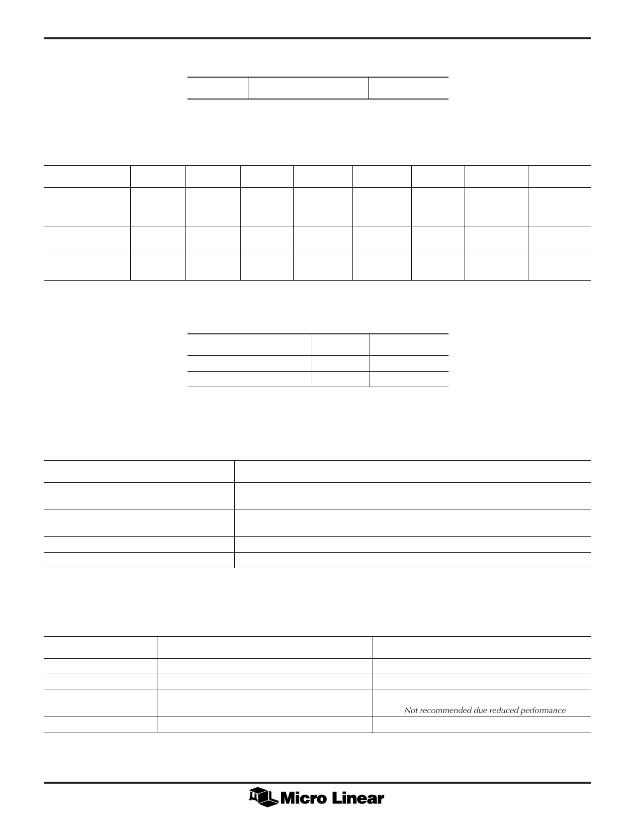
Table 1. Serial Data Format
BIT
Mode—Function
Value
Parallel Mode
Input Pin
D7
D6
Y+C or CV
Select
Y+C = 1
CV = 0
CI7/DI7
Adaption
Threshold
2
AT2 = 0
or 1
CI6/DI6
D5
Adaption
Threshold
1
AT1 = 0
or 1
CI5/DI5
D4
Adaption
Threshold
0
AT0 = 0
or 1
CI4/DI4
D3
Comb
Mode
1
CM1 = 0
or 1
CI3/DI3
D2
Comb
Mode
0
CM0 = 0
or 1
CI2/DI2
D1
D0
Square Pixel/
CCIR601
Select
Sq. Pixel = 1
CCIR601 = 0
CI1/DI1
PAL
or NTSC
Select
PAL = 1
NTSC = 0
CI0/DI0
Table 2. Control Register Format D[7:0] (Serial or Parallel Mode)
STANDARD/RATE
NTSC (fSC = 3.58MHz)
PAL (fSC = 4.43MHz)
CCIR601
13.5MHz
13.5MHz
SQUARE PIXEL
12.27MHz
14.75MHz
Table 3. Clock Frequency Requirements
ADAPTION THRESHOLD D[6,5,4]
000
001
010 to 110
111
ADAPTION THRESHOLD LEVEL
Automatic threshold for minimal comb artifact generation for various video
source material.
Threshold for computer graphics applications, minimizing dot crawl on
bold lettering.
Various degrees of thresholds.
Threshold for better reproduction of natural photographic images.
Table 4. Adaption Threshold Bit Table
COMB MODE, D[3,2]
00
01
10
11
8
NTSC
Y adaptive, C comb 100% active
Y adaptive, C adaptive
Y 100% comb active, C 100% comb active
Bandsplitting only (no combing)
PAL
Y adaptive, C adaptive
Y adaptive, C comb 100% active
Y 100% comb active, C 100% comb active
Not recommended due reduced performance
Bandsplitting only (no combing)
Table 5. Comb Mode Bit Table
Share Link: 