CXD2498 데이터 시트보기 (PDF) - Sony Semiconductor
부품명
상세내역
제조사
CXD2498 Datasheet PDF : 51 Pages
| |||
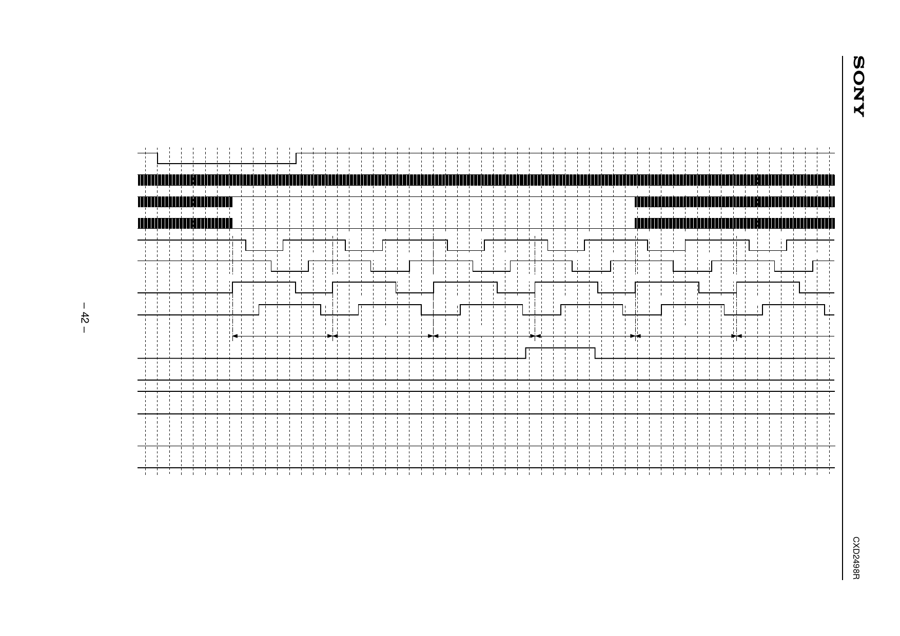
Chart-20 Horizontal Direction Timing Chart
(Frame shift: L)
MODE
Draft mode (AF1 and 2)
Applicable CCD image sensor
• ICX282
(3022)
0
HD
MCKO
4
H1A/B
H2A/B
V1A/B/C
V2
V3A/B/C
V4
SUB
PBLK
OBCLP
CLPDM
ID/EXP
WEN
50
100
150
200
250
300
350
400
450
500
550
62
398
426438 442
73
104
94
126
157
188
178
210
241
272
262
294
325
356
346
378
409
440
430
462
493
524
514
546
62
115
146
199
230
283
314
367
398
451
482
535
84
136
168
220
252
304
336
388
420
472
504
556
#1
#2
#3
#4
#5
#6
307
365
∗ The HD of this chart indicates the actual CXD2498R load timing.
∗ The numbers at the output pulse transition points indicate the count at the MCKO rise from the fall of HD.
∗ The HD fall period should be between approximately 2.8 to 12.0µs (when the drive frequency is 22.5MHz). This chart shows an period of 115ck (5.1µs). Internal SSG is at this timing.
∗ SUB is output at the timing shown above when output is controlled by the serial interface data.
∗ Frame shift of V1A/B/C, V2, V3A/B/C and V4 is performed up to 18H 2092ck (#276) in draft mode (AF1), 22H 2100ck (#420) in draft mode (AF2).
Share Link: 