EP1C12T173C6 데이터 시트보기 (PDF) - Altera Corporation
부품명
상세내역
제조사
EP1C12T173C6 Datasheet PDF : 104 Pages
| |||
Timing Model
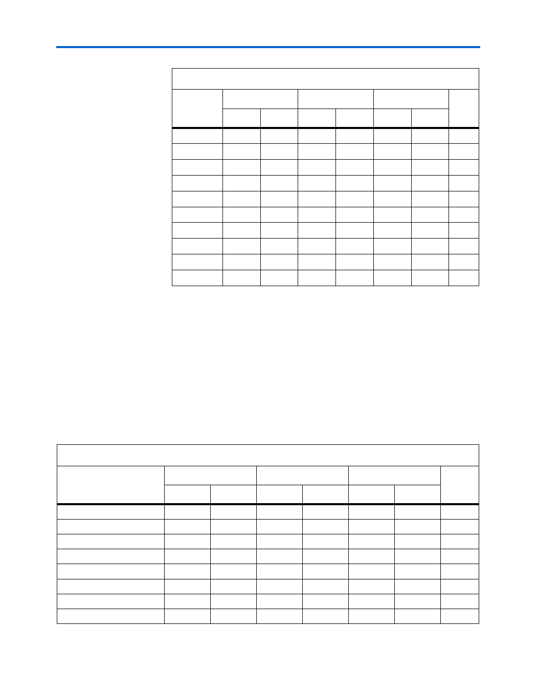
Table 4–39. EP1C20 Row Pin Global Clock External I/O Timing Parameters
Symbol
-6 Speed Grade -7 Speed Grade -8 Speed Grade
Unit
Min Max Min Max Min Max
tI N S U
2.417
2.779
3.140
ns
tI N H
0.000
0.000
0.000
ns
tO U T C O
2.000 3.724 2.000 4.282 2.000 4.843 ns
tX Z
3.645
4.191
4.740 ns
tZ X
3.645
4.191
4.740 ns
tI N S U P L L
1.417
1.629
1.840
ns
tI N H P L L
0.000
0.000
0.000
ns
tO U T C O P L L 0.500 1.667 0.500 1.917 0.500 2.169 ns
tX Z P L L
1.588
1.826
2.066 ns
tZ X P L L
1.588
1.826
2.066 ns
External I/O Delay Parameters
External I/O delay timing parameters for I/O standard input and output
adders and programmable input and output delays are specified by
speed grade independent of device density.
Tables 4–40 through 4–45 show the adder delays associated with column
and row I/O pins for all packages. If an I/O standard is selected other
than LVTTL 4 mA with a fast slew rate, add the selected delay to the
external tCO and tSU I/O parameters shown in Tables 4–25 through
4–28.
Table 4–40. Cyclone I/O Standard Column Pin Input Delay Adders (Part 1 of 2)
I/O Standard
LVCMOS
3.3-V LVTTL
2.5-V LVTTL
1.8-V LVTTL
1.5-V LVTTL
SSTL-3 class I
SSTL-3 class II
SSTL-2 class I
-6 Speed Grade
Min
Max
0
0
27
182
278
−250
−250
−278
-7 Speed Grade
Min
Max
0
0
31
209
319
−288
−288
−320
-8 Speed Grade
Unit
Min
Max
0
ps
0
ps
35
ps
236
ps
361
ps
−325
ps
−325
ps
−362
ps
Altera Corporation
January 2007
4–21
Preliminary
Share Link: 