AGL060V5-UC144ES 데이터 시트보기 (PDF) - Microsemi Corporation
부품명
상세내역
제조사
AGL060V5-UC144ES Datasheet PDF : 250 Pages
| |||
IGLOO Low Power Flash FPGAs
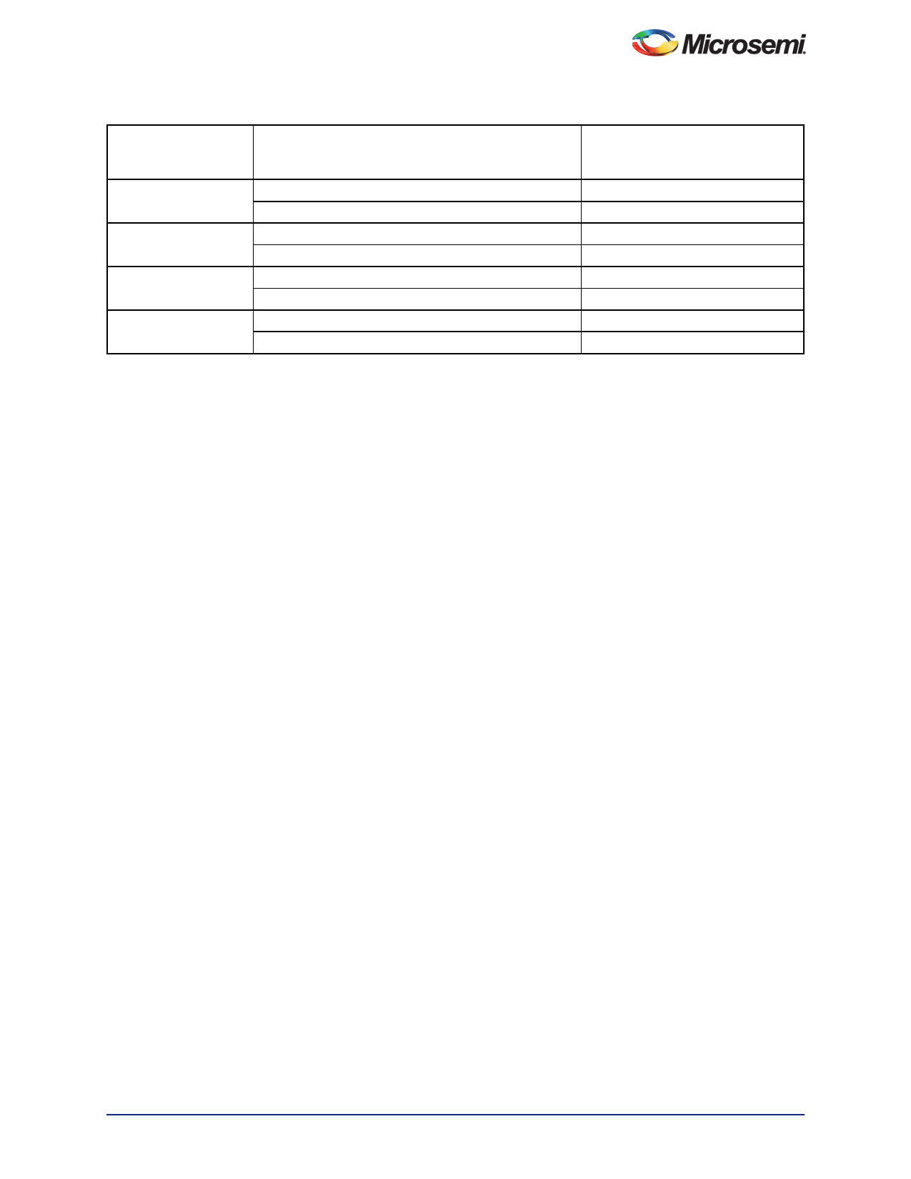
Table 2-4 • Overshoot and Undershoot Limits 1
VCCI
Average VCCI–GND Overshoot or
Undershoot Duration
as a Percentage of Clock Cycle2
Maximum Overshoot/
Undershoot2
2.7 V or less
10%
1.4 V
5%
1.49 V
3V
10%
1.1 V
5%
1.19 V
3.3 V
10%
0.79 V
5%
0.88 V
3.6 V
10%
0.45 V
5%
0.54 V
Notes:
1. Based on reliability requirements at junction temperature at 85°C.
2. The duration is allowed at one out of six clock cycles. If the overshoot/undershoot occurs at one out of two cycles, the
maximum overshoot/undershoot has to be reduced by 0.15 V.
3. This table does not provide PCI overshoot/undershoot limits.
I/O Power-Up and Supply Voltage Thresholds for Power-On Reset
(Commercial and Industrial)
Sophisticated power-up management circuitry is designed into every IGLOO device. These circuits
ensure easy transition from the powered-off state to the powered-up state of the device. The many
different supplies can power up in any sequence with minimized current spikes or surges. In addition, the
I/O will be in a known state through the power-up sequence. The basic principle is shown in Figure 2-1
on page 2-4 and Figure 2-2 on page 2-5.
There are five regions to consider during power-up.
IGLOO I/Os are activated only if ALL of the following three conditions are met:
1. VCC and VCCI are above the minimum specified trip points (Figure 2-1 on page 2-4 and
Figure 2-2 on page 2-5).
2. VCCI > VCC – 0.75 V (typical)
3. Chip is in the operating mode.
VCCI Trip Point:
Ramping up (V5 devices): 0.6 V < trip_point_up < 1.2 V
Ramping down (V5 Devices): 0.5 V < trip_point_down < 1.1 V
Ramping up (V2 devices): 0.75 V < trip_point_up < 1.05 V
Ramping down (V2 devices): 0.65 V < trip_point_down < 0.95 V
VCC Trip Point:
Ramping up (V5 devices): 0.6 V < trip_point_up < 1.1 V
Ramping down (V5 devices): 0.5 V < trip_point_down < 1.0 V
Ramping up (V2 devices): 0.65 V < trip_point_up < 1.05 V
Ramping down (V2 devices): 0.55 V < trip_point_down < 0.95 V
VCC and VCCI ramp-up trip points are about 100 mV higher than ramp-down trip points. This specifically
built-in hysteresis prevents undesirable power-up oscillations and current surges. Note the following:
• During programming, I/Os become tristated and weakly pulled up to VCCI.
• JTAG supply, PLL power supplies, and charge pump VPUMP supply have no influence on I/O
behavior.
Revision 23
2-3
Share Link: 