74ACTQ00PC 데이터 시트보기 (PDF) - Fairchild Semiconductor
부품명
상세내역
제조사
74ACTQ00PC Datasheet PDF : 7 Pages
| |||
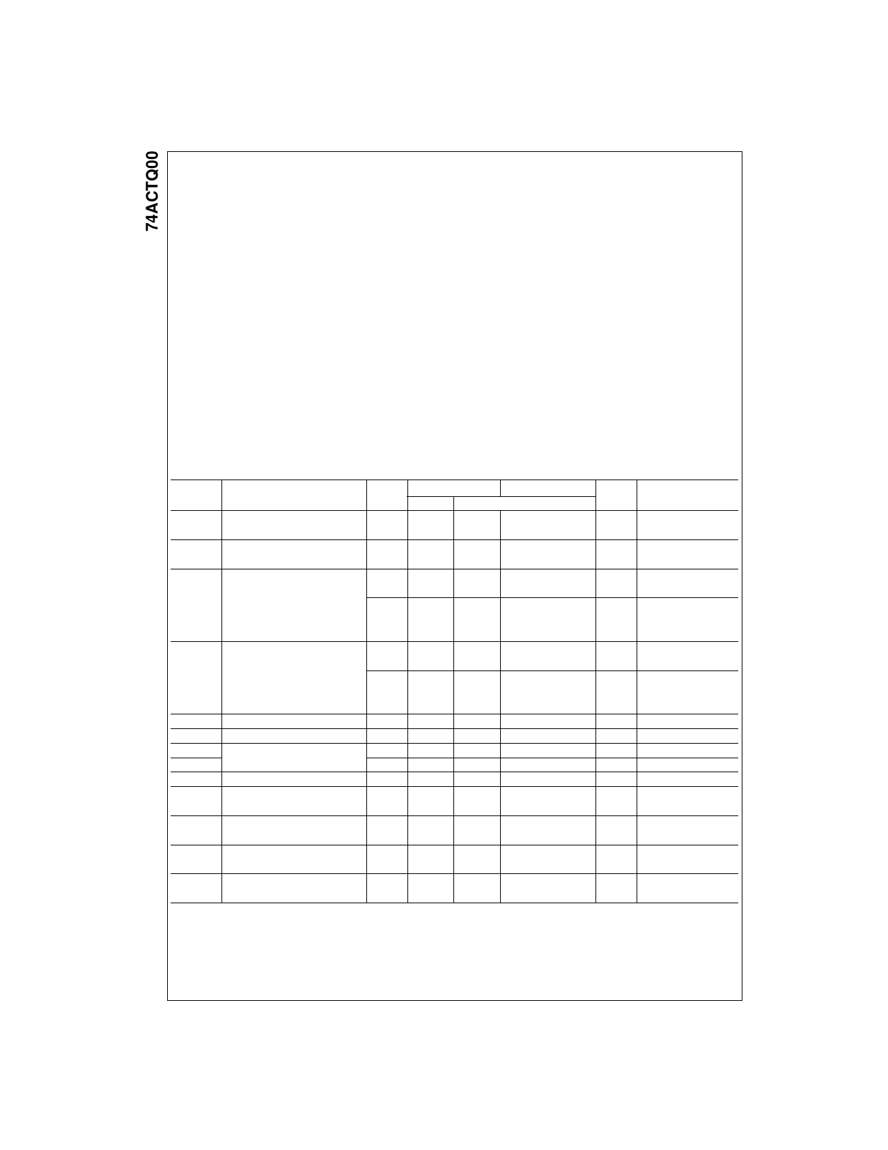
Absolute Maximum Ratings(Note 1)
Supply Voltage (VCC)
DC Input Diode Current (IIK)
VI 0.5V
VI VCC 0.5V
DC Input Voltage (VI)
DC Output Diode Current (IOK)
VO 0.5V
VO VCC 0.5V
DC Output Voltage (VO)
DC Output Source
or Sink Current (IO)
DC VCC or Ground Current
per Output Pin (ICC or IGND)
Storage Temperature (TSTG)
DC Latch-up Source
0.5V to 7.0V
20 mA
20 mA
0.5V to VCC 0.5V
20 mA
20 mA
0.5V to VCC 0.5V
r50 mA
r50 mA
65qC to 150qC
or Sink Current
Junction Temperature (TJ)
PDIP
r300 mA
140qC
Recommended Operating
Conditions
Supply Voltage (VCC)
Input Voltage (VI)
Output Voltage (VO)
Operating Temperature (TA)
Minimum Input Edge Rate ('V/'t)
4.5V to 5.5V
0V to VCC
0V to VCC
40qC to 85qC
VIN from 0.8V to 2.0V
125 mV/ns
VCC @ 4.5V, 5.5V
Note 1: Absolute maximum ratings are those values beyond which damage
to the device may occur. The databook specifications should be met, with-
out exception, to ensure that the system design is reliable over its power
supply, temperature, and output/input loading variables. Fairchild does not
recommend operation outside databook specifications.
DC Electrical Characteristics
Symbol
Parameter
VCC
TA 25qC
TA 40qC to 85qC Units
(V)
Typ
Guaranteed Limits
Conditions
VIH
Minimum HIGH Level
Input Voltage
VIL
Maximum LOW Level
Input Voltage
VOH
Minimum HIGH Level
Output Voltage
4.5
1.5
2.0
2.0
V
VOUT 0.1V
5.5
1.5
2.0
2.0
or VCC 0.1V
4.5
1.5
0.8
0.8
V
VOUT 0.1V
5.5
1.5
0.8
0.8
or VCC 0.1V
4.5
4.49
4.4
4.4
5.5
5.49
5.4
5.4
V
IOUT 50 PA
VOL
Maximum LOW Level
Output Voltage
4.5
3.86
5.5
4.86
4.5
0.001
0.1
5.5
0.001
0.1
3.76
4.76
0.1
0.1
VIN VIL or VIH
V
IOH 24 mA
IOH 24 mA (Note 2)
V
IOUT 50 PA
IIN
ICCT
IOLD
IOHD
ICC
VOLP
VOLV
VIHD
4.5
0.36
5.5
0.36
Maximum Input Leakage Current
5.5
r0.1
Maximum ICC/Input
Minimum Dynamic
5.5
0.6
5.5
Output Current (Note 3)
5.5
Maximum Quiescent Supply Current 5.5
2.0
Quiet Output Maximum Dynamic
5.0
1.1
1.5
VOL
Quiet Output Minimum Dynamic
VOL
Minimum HIGH Level
5.0
0.6
1.2
5.0
1.9
2.2
Dynamic Input Voltage
0.44
0.44
r1.0
1.5
75
75
20.0
VIN VIL or VIH
V
IOL 24 mA
IOL 24 mA (Note 2)
PA VI VCC, GND
mA V I VCC 2.1V
mA VOLD 1.65V Max
mA VOHD 3.85V Min
PA VIN VCC or GND
V Figure 1, Figure 2
(Note 4)(Note 5)
Figure 1, Figure 2
V
(Note 4)(Note 5)
V (Note 4)(Note 6)
VILD
Maximum LOW Level
Dynamic Input Voltage
5.0
1.2
0.8
V (Note 4)(Note 6)
Note 2: All outputs loaded; thresholds on input associated with output under test.
Note 3: Maximum test duration 2.0 ms, one output loaded at a time.
Note 4: DIP package.
Note 5: Max number of outputs defined as (n). Data inputs are 0V to 3V. One output @ GND.
Note 6: Max number of data inputs (n) switching. (n1) inputs switching 0V to 3V. Input-under-test switching: 3V to threshold (VILD),
0V to threshold (VIHD), f 1 MHz.
www.fairchildsemi.com
2
Share Link: 