LT1886CS8 데이터 시트보기 (PDF) - Linear Technology
부품명
상세내역
제조사
LT1886CS8 Datasheet PDF : 16 Pages
| |||
LT1886
APPLICATIO S I FOR ATIO
For example, reducing RBT by a factor of n = 4, and with an
amplifer gain of (1 + RF/RG) = 10 requires that RP2/RP1
=␣ 12.3.
Note that the overall gain is increased:
[ ] [ ] Vo
Vi
=
RP2 / (RP2 + RP1)
(1+ 1/ n) / (1+ RF /RG) − RP1 / (RP2 + RP1)
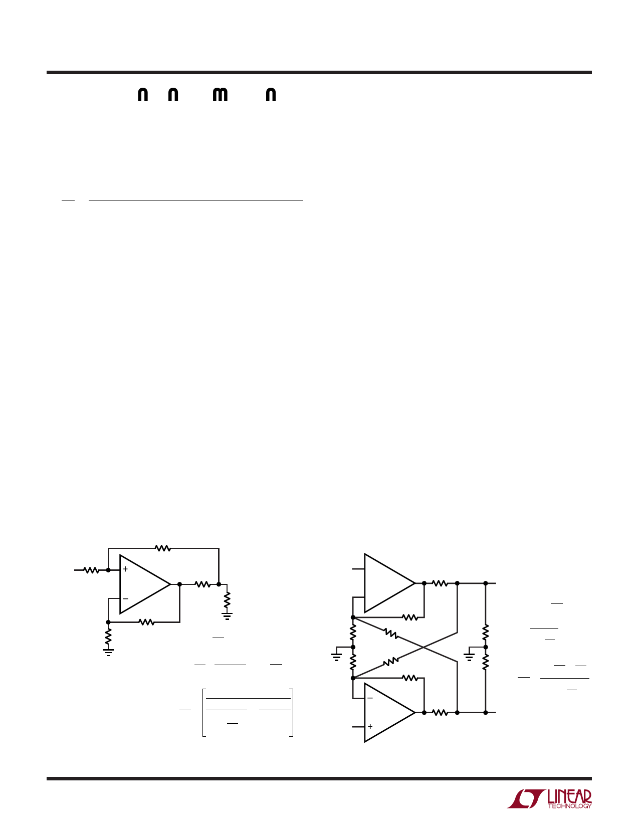
A simpler method of using positive feedback to reduce the
back-termination is shown in Figure 8. In this case, the
drivers are driven differentially and provide complemen-
tary outputs. Grounding the inputs, we see there is invert-
ing gain of –RF/RP from –Vo to Va
Va = Vo (RF/RP)
and assuming RP >> RL, we require
Va = Vo (1 – 1/n)
solving
RF/RP = 1 – 1/n
So to reduce the back-termination by a factor of 3 choose
RF/RP = 2/3. Note that the overall gain is increased to:
Vo/Vi = (1 + RF/RG + RF/RP)/[2(1 – RF/RP)]
ADSL Driver Requirements
The LT1886 is an ideal choice for ADSL upstream (CPE)
modems. The key advantages are: ±200mA output drive
RP2
RP1
+
Vi
VP
–
RF
RG
Va RBT Vo
RL
1886 F07
FOR RBT = RL
n
( ) ( ) 1 + RF
RG
RP1
1
=1–
RP1 + RP2
n
Vo =
Vi
RP2/(RP2 + RP1)
1 + 1/n
( ) 1 + RF
RG
– RP1
RP2 + RP1
Figure 7. Back-Termination Using Positive Feedback
with only 1.7V worst-case total supply voltage headroom,
high bandwidth, which helps achieve low distortion, low
quiescent supply current of 7mA per amplifier and a
space-saving, thermally enhanced SO-8 package.
An ADSL remote terminal driver must deliver an average
power of 13dBm (20mW) into a 100Ω line. This corre-
sponds to 1.41VRMS into the line. The DMT-ADSL peak-to-
average ratio of 5.33 implies voltage peaks of 7.53V into
the line. Using a differential drive configuration and trans-
former coupling with standard back-termination, a trans-
former ratio of 1:2 is well suited. This is shown on the front
page of this data sheet along with the distortion perfor-
mance vs line voltage at 200kHz, which is beyond ADSL
requirements. Note that the distortion is better than
–73dBc for all swings up to 16VP-P into the line. The gain
of this circuit from the differential inputs to the line voltage
is 10. Lower gains are easy to implement using the
compensation techniques of Figure 5. Table 2 shows the
drive requirements for this standard circuit.
The above design is an excellent choice for desktop
applications and draws typically 550mW of power. For
portable applications, power savings can be achieved by
reducing the back-termination resistor using positive feed-
back as shown in Figure 9. The overall gain of this circuit
is also 10, but the power consumption has been reduced
to 350mW, a savings of 36% over the previous design.
Note that the reduction of the back-termination resistor
has allowed use of a 1:1 transformer ratio.
Vi +
–
Va RBT
RF
RG
RP
RP
RG
RF
–
+
–Vi
RBT
–Va
Vo
FOR RBT = RL
n
RL
n= 1
1 – RF
RP
RL
1 + RF + RF
Vo =
Vi
RG RP
( ) 2 1 – RF
RP
–Vo
1886 F08
Figure 8. Back-Termination Using Differential Positive Feedback
12
Share Link: 