MC74VHC125 데이터 시트보기 (PDF) - ON Semiconductor
부품명
상세내역
제조사
MC74VHC125 Datasheet PDF : 8 Pages
| |||
MC74VHC125
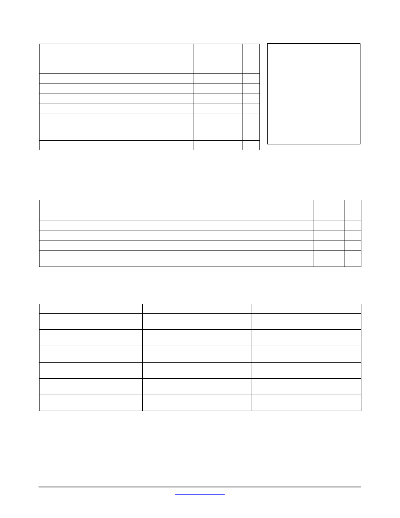
ÎÎÎÎÎÎÎÎÎÎÎÎÎÎÎÎÎÎÎÎÎÎÎ MAXIMUM RATINGS
ÎÎÎÎÎÎÎÎÎÎÎÎÎÎÎÎÎÎÎÎÎÎÎ Symbol
Parameter
ÎÎÎÎÎÎÎÎÎÎÎÎÎÎÎÎÎÎÎÎÎÎÎ VCC DC Supply Voltage
ÎÎÎÎÎÎÎÎÎÎÎÎÎÎÎÎÎÎÎÎÎÎÎ Vin DC Input Voltage
ÎÎÎÎÎÎÎÎÎÎÎÎÎÎÎÎÎÎÎÎÎÎÎ Vout DC Output Voltage
ÎÎÎÎÎÎÎÎÎÎÎÎÎÎÎÎÎÎÎÎÎÎÎ IIK
Input Diode Current
ÎÎÎÎÎÎÎÎÎÎÎÎÎÎÎÎÎÎÎÎÎÎÎ IOK Output Diode Current
ÎÎÎÎÎÎÎÎÎÎÎÎÎÎÎÎÎÎÎÎÎÎÎ Iout DC Output Current, per Pin
ÎÎÎÎÎÎÎÎÎÎÎÎÎÎÎÎÎÎÎÎÎÎÎ ICC DC Supply Current, VCC and GND Pins
ÎÎÎÎÎÎÎÎÎÎÎÎÎÎÎÎÎÎÎÎÎÎÎ PD Power Dissipation in Still Air, SOIC Packages†
TSSOP Package†
ÎÎÎÎÎÎÎÎÎÎÎÎÎÎÎÎÎÎÎÎÎÎÎÎÎÎÎÎÎÎÎÎÎÎÎÎÎÎÎÎÎÎÎÎÎÎ Tstg StorageTemperature
Value
Unit
–0.5 to +7.0
V
–0.5 to +7.0
V
–0.5 to VCC +0.5 V
− 20
mA
$ 20
mA
$ 25
mA
$ 50
mA
500
mW
450
–65 to +150
°C
Stresses exceeding those listed in the Maximum Ratings table may damage the device. If any
of these limits are exceeded, device functionality should not be assumed, damage may occur
and reliability may be affected.
†Derating − SOIC Packages: – 7 mW/°C from 65° to 125°C
TSSOP Package: − 6.1 mW/°C from 65° to 125°C
This device contains protection
circuitry to guard against damage
due to high static voltages or elec-
tric fields. However, precautions
must be taken to avoid applications
of any voltage higher than maxim-
um rated voltages to this high−im-
pedance circuit. For proper opera-
tion, Vin and Vout should be con-
strained to the range GND v (Vin
or Vout) v VCC.
Unused inputs must always be
tied to an appropriate logic voltage
level (e.g., either GND or VCC). Un-
used outputs must be left open.
RECOMMENDED OPERATING CONDITIONS
ÎÎÎÎÎÎÎÎÎÎÎÎÎÎÎÎÎÎÎÎÎÎÎÎÎÎÎÎÎÎÎÎÎ Symbol
Parameter
Min
Max
Unit
ÎÎÎÎÎÎÎÎÎÎÎÎÎÎÎÎÎÎÎÎÎÎÎÎÎÎÎÎÎÎÎÎÎ VCC DCSupplyVoltage
2.0
5.5
V
ÎÎÎÎÎÎÎÎÎÎÎÎÎÎÎÎÎÎÎÎÎÎÎÎÎÎÎÎÎÎÎÎÎ Vin DCInputVoltage
0
5.5
V
ÎÎÎÎÎÎÎÎÎÎÎÎÎÎÎÎÎÎÎÎÎÎÎÎÎÎÎÎÎÎÎÎÎ Vout DCOutputVoltage
0
VCC
V
ÎÎÎÎÎÎÎÎÎÎÎÎÎÎÎÎÎÎÎÎÎÎÎÎÎÎÎÎÎÎÎÎÎ TA Operating Temperature, All Package Types
−55
+125
°C
ÎÎÎÎÎÎÎÎÎÎÎÎÎÎÎÎÎÎÎÎÎÎÎÎÎÎÎÎÎÎÎÎÎÎÎÎÎÎÎÎÎÎÎÎÎÎÎÎÎÎÎÎÎÎÎÎÎÎÎÎÎÎÎÎÎÎ tr,tf InputRiseandFallTime
VCC = 3.3 V $0.3 V
VCC =5.0 V $0.5 V
0
100
ns/V
0
20
ÎÎÎÎÎÎÎÎÎÎÎÎÎÎÎÎÎÎÎÎÎÎÎÎÎÎÎÎÎÎÎÎÎ Functional operation above the stresses listed in the Recommended Operating Ranges is not implied. Extended exposure to stresses beyond
the Recommended Operating Ranges limits may affect device reliability.
ORDERING INFORMATION
Device
MC74VHC125DG
Package
SOIC−14
(Pb−Free)
Shipping†
55 Units / Rail
NLV74VHC125DG*
SOIC−14
(Pb−Free)
55 Units / Rail
MC74VHC125DR2G
SOIC−14
(Pb−Free)
2500 / Tape & Reel
NLV74VHC125DR2G*
SOIC−14
(Pb−Free)
2500 / Tape & Reel
MC74VHC125DTR2G
TSSOP−14
(Pb−Free)
2500 / Tape & Reel
NLV74VHC125DTR2G*
TSSOP−14
(Pb−Free)
2500 / Tape & Reel
†For information on tape and reel specifications, including part orientation and tape sizes, please refer to our Tape and Reel Packaging
Specifications Brochure, BRD8011/D.
*NLV Prefix for Automotive and Other Applications Requiring Unique Site and Control Change Requirements; AEC−Q100 Qualified and PPAP
Capable.
www.onsemi.com
2
Share Link: 