AD8304 데이터 시트보기 (PDF) - Analog Devices
부품명
상세내역
제조사
AD8304 Datasheet PDF : 21 Pages
| |||
AD8304
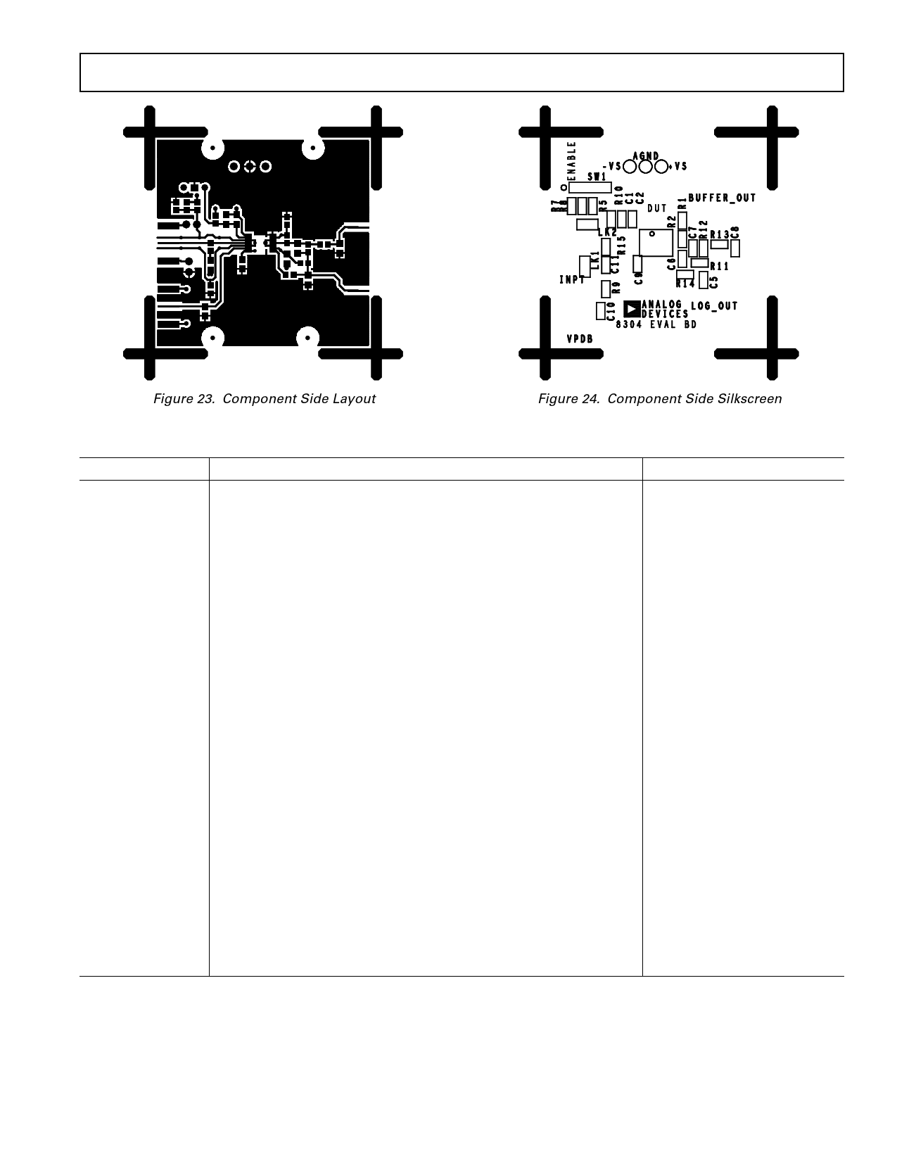
Figure 23. Component Side Layout
Figure 24. Component Side Silkscreen
Component
VP, VN, AGND
SW1, R10
R1, R2
R3, R4
R5, R6, R7, R8, R9
C1, C2, C3, C4, C9
Table V. Evaluation Board Configuration Options
Function
Positive and Negative Supply and Ground Pins
Device Enable: When SW1 is in the “0” position, the PWDN Pin is
connected to ground and the AD8304 is in its normal operating mode.
Buffer Amplifier Gain/Slope Adjustment: The logarithmic slope
of the AD8304 can be altered using the buffer’s gain-setting resistors,
R1 and R2.
Intercept Adjustment: A dc offset can be applied to the input term-
inals of the buffer amplifier to adjust the effective logarithmic intercept.
Bias Adjustment: The voltage on the VSUM and INPT Pins can be
altered using appropriate resistor values. R9 is populated with a decoup-
ling capacitor to reduce noise pickup. The decoupling capacitor can be
removed when a fixed bias is applied to VSUM.
Supply Decoupling Capacitors
C10
Photodiode Biaser Decoupling: Provides high frequency decoupling
of the adaptive bias output at Pin VPDB.
C5, C6, C7, C8, R11, Output Filtering: Allows implementation of a variety of filter config-
R12, R13, R14
urations, from simple RC low-pass filters to three-pole Sallen and Key.
R15, C11
LK1, LK2
Input Filtering: Provides essential HF compensation at the input
Pin INPT.
Guard/Shield Options: The shells of the SMA connectors used
for the input and the photodiode bias can be set to the voltage on the
VSUM Pin or connected to ground.
Default Condition
Not Applicable
SW1 = Installed
R10 = 10 kΩ (Size 0603)
R1 = Open (Size 0603)
R2 = 0 Ω (Size 0603)
R3 = Open (Size 0603)
R4 = Open (Size 0603)
R5 = R6 = Open (Size 0603)
R7 = R8 = Open (Size 0603)
R9 = 0.1 µF (Size 0603)
C1 = C4 = 0.1 µF (Size 0603)
C2 = C3 = 1 nF (Size 0603)
C9 = 10 nF (Size 0603)
C10 = 0.1 µF (Size 0603)
R11 = R13 = 0 Ω (Size 0603)
R12 = Open (Size 0603)
R14 = 0 Ω (Size 0603)
C5 = C6 = Open (Size 0603)
C7 = C8 = Open (Size 0603)
R15 = 750 Ω (Size 0603)
C11 = 1 nF (Size 0603)
LK1 = Installed
LK2 = Open
REV. A
–19–
Share Link: 