74LV132 데이터 시트보기 (PDF) - Philips Electronics
부품명
상세내역
제조사
74LV132 Datasheet PDF : 12 Pages
| |||
Philips Semiconductors
Quad 2-input NAND Schmitt-trigger
Product specification
74LV132
AC CHARACTERISTICS
GND = 0V; tr = tf = 2.5ns; CL = 50pF
SYMBOL
PARAMETER
WAVEFORM
CONDITION
VCC(V)
1.2
tPHL/tPLH
Propagation delay
nA, nB, to nY
Figure 6
2.0
2.7
3.0 to 3.6
4.5 to 5.5
NOTES:
1. Unless otherwise stated, all typical values are at Tamb = 25°C.
2. Typical value measured at VCC = 3.3V.
3. Typical value measured at VCC = 5.0V.
TRANSFER CHARACTERISTIC WAVEFORMS
LIMITS
–40 to +85°C
MIN TYP1 MAX
–
65
–
–
18
34
–
15
24
–
122
20
–
9.02
14
–40 to +125°C
MIN MAX
–
–
–
43
–
30
–
25
–
17
UNIT
ns
VO
VH
VT–
VT+
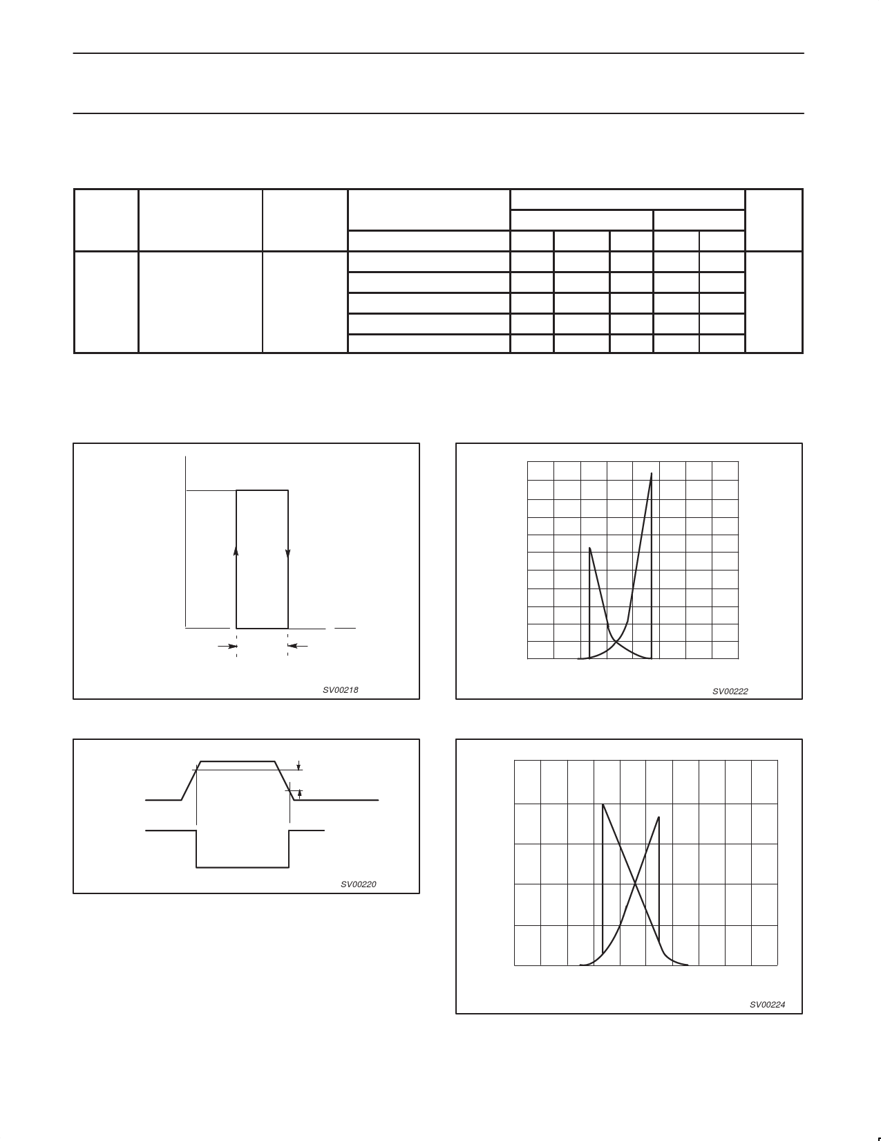
SV00218
Figure 1. Transfer characteristic.
10
ICC
(µA)
8
6
4
2
0
0
0.3
0.6
0.9
1.2
VIN (V)
SV00222
Figure 3. Typical LV132 transfer characteristics; VCC = 1.2V.
VT+
VI
VM
VT–
VO
SV00220
Figure 2. Definition of VT+, VT– and VH; where VT+ and VT– are
between limits of 20% and 70%.
100
ICC
(µA)
80
60
40
20
0
0
0.4
0.8
1.2
1.6
2.0
VIN (V)
SV00224
Figure 4. Typical LV132 transfer characteristics; VCC = 2.0V.
1998 Apr 28
6
Share Link: 