AD7147 데이터 시트보기 (PDF) - Analog Devices
부품명
상세내역
제조사
AD7147 Datasheet PDF : 71 Pages
| |||
AD7147
Data Sheet
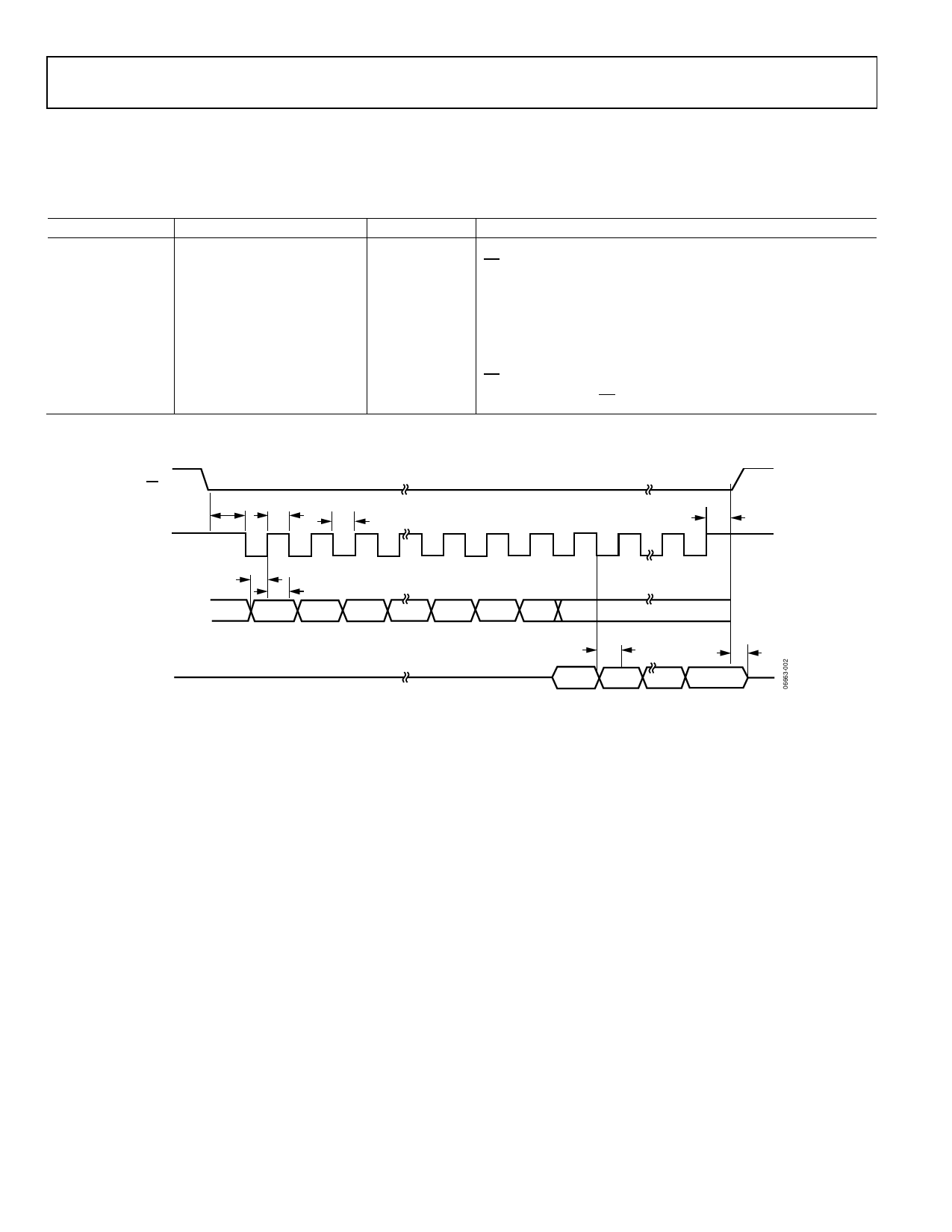
SPI TIMING SPECIFICATIONS (AD7147)
TA = −40°C to +85°C, sample tested at 25°C to ensure compliance. VDRIVE = 1.65 V to 3.6 V, and VCC = 2.6 V to 3.6 V, unless otherwise
noted. All input signals are specified with tR = tF = 5 ns (10% to 90% of VCC) and timed from a voltage level of 1.6 V.
Table 4. SPI Timing Specifications
Parameter
Limit
fSCLK
5
t1
5
t2
20
t3
20
t4
15
t5
15
t6
20
t7
16
t8
15
Unit
MHz max
ns min
ns min
ns min
ns min
ns min
ns max
ns max
ns min
Description
SCLK frequency
CS falling edge to first SCLK falling edge
SCLK high pulse width
SCLK low pulse width
SDI setup time
SDI hold time
SDO access time after SCLK falling edge
CS rising edge to SDO high impedance
SCLK rising edge to CS high
SPI Timing Diagram
CS
SCLK
SDI
SDO
t1
t2
1
t4
t5
MSB
t3
2
3
15
16
1
2
LSB
t6
MSB
Figure 2. SPI Detailed Timing Diagram
t8
15
16
t7
LSB
Rev. E | Page 6 of 70
Share Link: 