ADG5208 데이터 시트보기 (PDF) - Analog Devices
부품명
상세내역
제조사
ADG5208 Datasheet PDF : 24 Pages
| |||
ADG5208/ADG5209
PIN CONFIGURATIONS AND FUNCTION DESCRIPTIONS
Data Sheet
A0 1
16 A1
EN 2
15 A2
VSS 3 ADG5208 14 GND
S1 4 TOP VIEW 13 VDD
S2 5 (Not to Scale) 12 S5
S3 6
11 S6
S4 7
10 S7
D8
9 S8
Figure 2. ADG5208 Pin Configuration (TSSOP)
VSS 1
S1 2
S2 3
S3 4
ADG5208
TOP VIEW
(Not to Scale)
12 GND
11 VDD
10 S5
9 S6
NOTES
1. THE EXPOSED PAD IS CONNECTED INTERNALLY. FOR
INCREASED RELIABILITY OF THE SOLDER JOINTS AND
MAXIMUM THERMAL CAPABILITY, IT IS RECOMMENDED
THAT THE PAD BE SOLDERED TO THE SUBSTRATE, VSS.
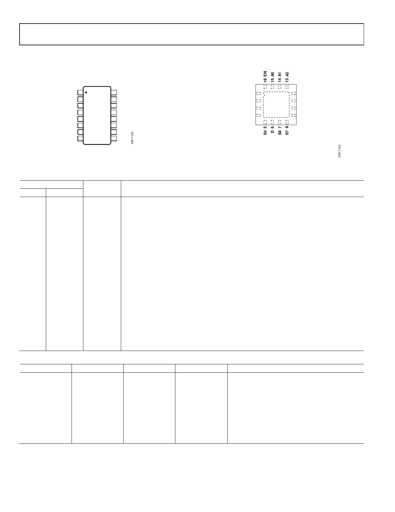
Figure 3. ADG5208 Pin Configuration (LFCSP)
Table 8. ADG5208 Pin Function Descriptions
Pin No.
TSSOP LFCSP
Mnemonic Description
1
15
A0
Logic Control Input.
2
16
EN
Active High Digital Input. When low, the device is disabled and all switches are off. When high, the
Ax logic inputs determine the on switches.
3
1
VSS
Most Negative Power Supply Potential. In single-supply applications, this pin can be connected
to ground.
4
2
S1
Source Terminal 1. This pin can be an input or an output.
5
3
S2
Source Terminal 2. This pin can be an input or an output.
6
4
S3
Source Terminal 3. This pin can be an input or an output.
7
5
S4
Source Terminal 4. This pin can be an input or an output.
8
6
D
Drain Terminal. This pin can be an input or an output.
9
7
S8
Source Terminal 8. This pin can be an input or an output.
10
8
S7
Source Terminal 7. This pin can be an input or an output.
11
9
S6
Source Terminal 6. This pin can be an input or an output.
12
10
S5
Source Terminal 5. This pin can be an input or an output.
13
11
VDD
Most Positive Power Supply Potential.
14
12
GND
Ground (0 V) Reference.
15
13
A2
Logic Control Input.
16
14
A1
Logic Control Input.
EP
Exposed Pad The exposed pad is connected internally. For increased reliability of the solder joints and
maximum thermal capability, it is recommended that the pad be soldered to the substrate, VSS.
Table 9. ADG5208 Truth Table
A2
A1
A0
EN
On Switch
X1
X1
X1
0
None
0
0
0
1
1
0
0
1
1
2
0
1
0
1
3
0
1
1
1
4
1
0
0
1
5
1
0
1
1
6
1
1
0
1
7
1
1
1
1
8
1 X is don’t care.
Rev. C | Page 10 of 24
Share Link: 