ADIS16223CMLZ 데이터 시트보기 (PDF) - Analog Devices
부품명
상세내역
제조사
ADIS16223CMLZ Datasheet PDF : 20 Pages
| |||
Data Sheet
ADIS16223
THEORY OF OPERATION
The ADIS16223 is a tri-axial, wide bandwidth, digital acceleration
sensor for vibration analysis. This sensing system collects data
autonomously and makes it available to any processor system that
TRIAXIAL
MEMS
SENSOR
CAPTURE
BUFFER
OUTPUT
REGISTERS
supports a 4-wire serial peripheral interface (SPI).
SENSING ELEMENT
Digital vibration sensing in the ADIS16223 starts with a wide
TEMP
SENSOR
ADC
CONTROLLER
CONTROL
REGISTERS
bandwidth MEMS accelerometer core on each axis, which provides
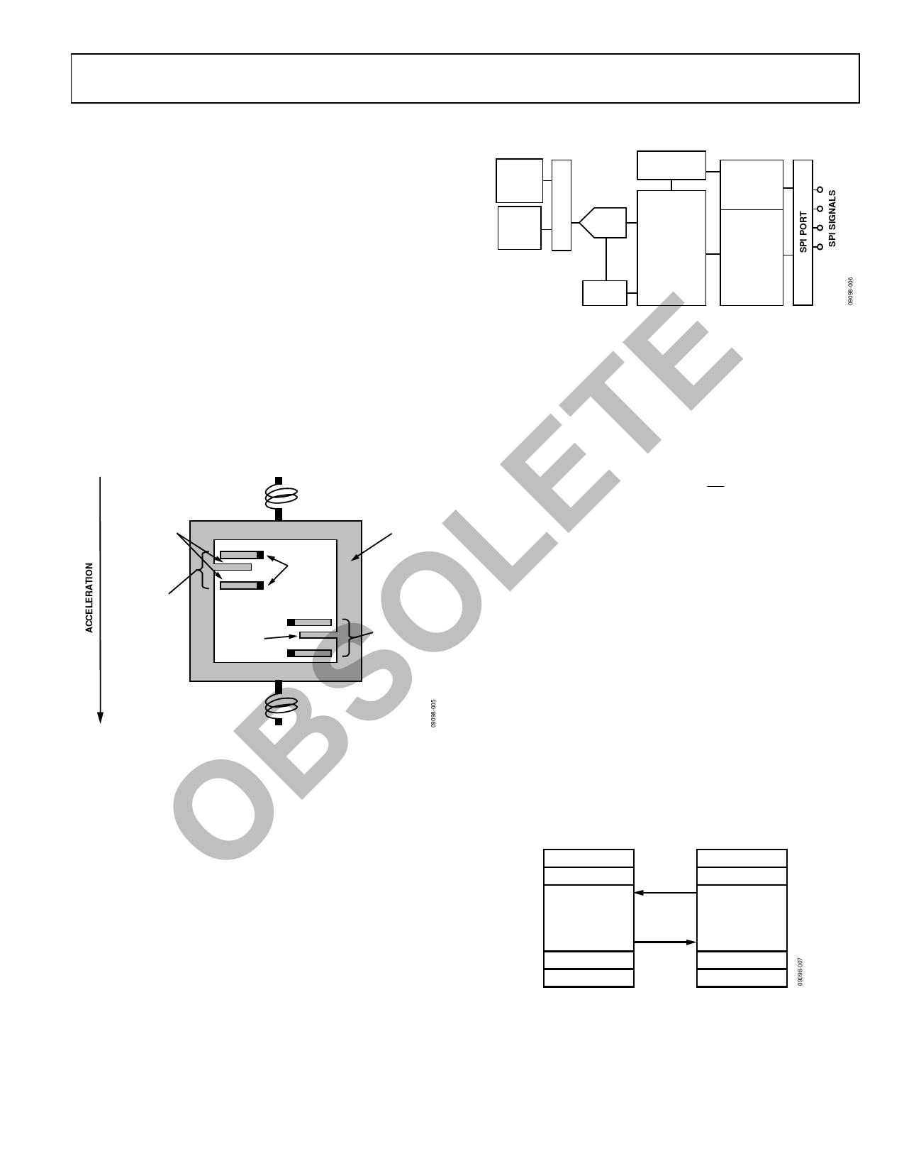
a linear motion-to-electrical transducer function. Figure 5 provides
CLOCK
a basic physical diagram of the sensing element and its response
Figure 6. Simplified Sensor Signal Processing Diagram
to linear acceleration. It uses a fixed frame and a moving frame
to form a differential capacitance network that responds to linear
acceleration. Tiny springs tether the moving frame to the fixed
frame and govern the relationship between acceleration and
physical displacement. A modulation signal on the moving plate
E feeds through each capacitive path into the fixed frame plates and
into a demodulation circuit, which produces the electrical signal
that is proportional to the acceleration acting on the device.
T ANCHOR
PLATE
CAPACITORS
MOVABLE
FRAME
LE UNIT SENSING
CELL
FIXED
PLATES
MOVING
PLATE
UNIT
FORCING
CELL
O ANCHOR
S Figure 5. MEMS Sensor Diagram
DATA SAMPLING AND PROCESSING
The analog acceleration signal from each sensor feeds into an
B analog-to-digital (ADC) converter stage, which passes digitized
data into the controller. The controller processes the acceleration
data, stores it in the capture buffer, and manages access to it using
O the SPI/register user interface. Processing options include offset
USER INTERFACE
SPI Interface
The user registers manage user access to both sensor data and
configuration inputs. Each 16-bit register has its own unique bit
assignment and two addresses: one for its upper byte and one for
its lower byte. Table 8 provides a memory map for each register,
along with its function and lower byte address. Each data
collection and configuration command both use the SPI, which
consists of four wires. The chip select (CS) signal activates the
SPI interface and the serial clock (SCLK) synchronizes the serial
data lines. Input commands clock into the DIN pin, one bit at a
time, on the SCLK rising edge. Output data clocks out of the
DOUT pin on the SCLK falling edge. As a SPI slave device, the
DOUT contents reflect the information requested using a DIN
command.
Dual Memory Structure
The user registers provide addressing for all input/output operations
on the SPI interface. The control registers use a dual memory
structure. The SRAM controls operation while the part is on and
facilitates all user configuration inputs. The flash memory provides
nonvolatile storage for control registers that have flash backup
(see Table 8). Storing configuration data in the flash memory
requires a manual, flash update command (GLOB_CMD[12] = 1,
DIN = 0xBF10). When the device powers on or resets, the flash
memory contents load into the SRAM, and then the device starts
producing data according to the configuration in the control
registers.
MANUAL
adjustment, filtering, and checking for preset alarm conditions.
FLASH
BACKUP
NONVOLATILE
FLASH MEMORY
(NO SPI ACCESS)
VOLATILE
SRAM
SPI ACCESS
START-UP
RESET
Figure 7. SRAM and Flash Memory Diagram
Rev. A | Page 7 of 20
Share Link: 