APW7073AKE-TRG 데이터 시트보기 (PDF) - Anpec Electronics
부품명
상세내역
제조사
APW7073AKE-TRG Datasheet PDF : 20 Pages
| |||
APW7073A
Application Information (Cont.)
PWM Compensation (Cont.)
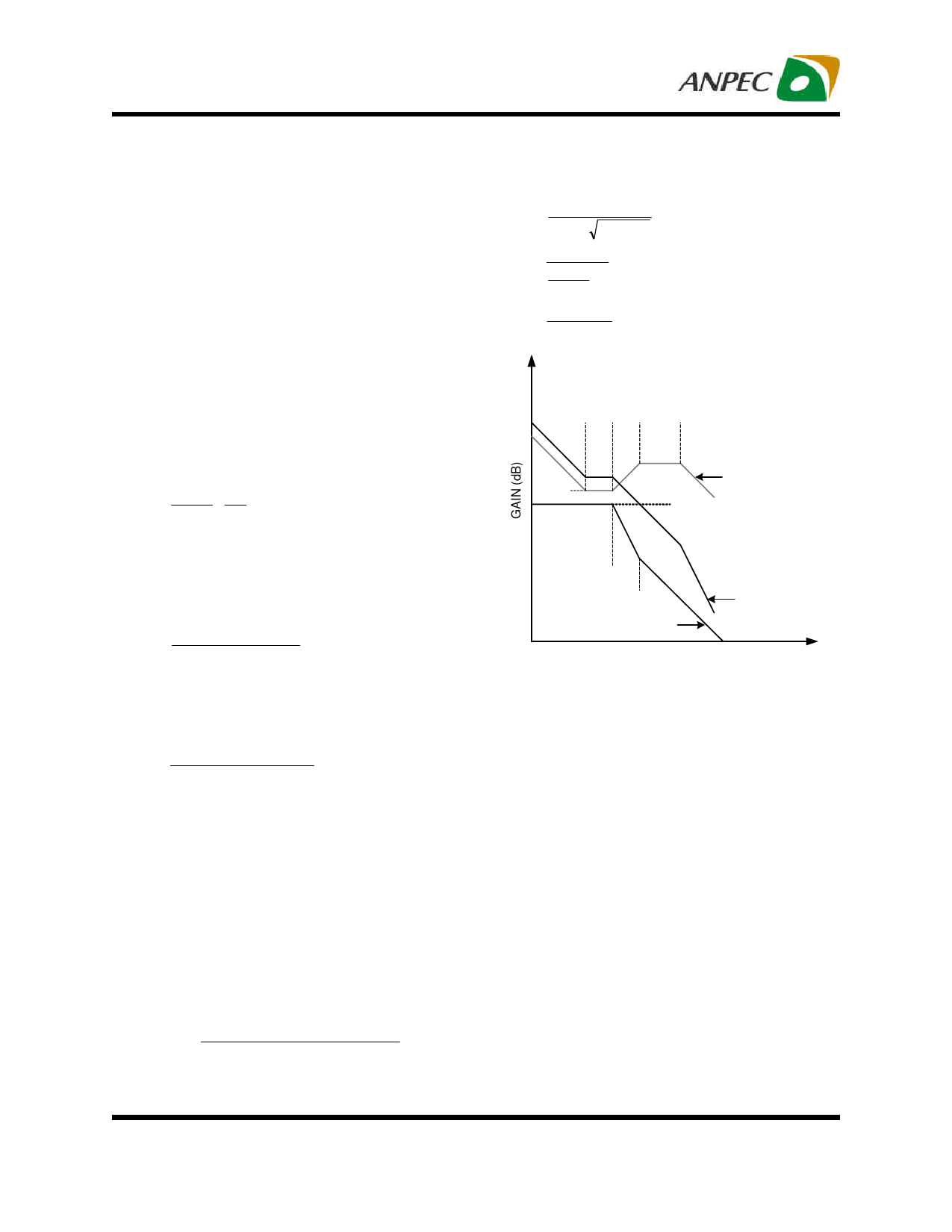
The closed loop gain of the converter can be written as:
GAINLC X GAINPWM X GAINAMP
Figure 9. shows the asymptotic plot of the closed loop
converter gain, and the following guidelines will help to
design the compensation network. Using the below
guidelines should give a compensation similar to the
curve plotted. A stable closed loop has a -20dB/ decade
slope and a phase margin greater than 45 degree.
1. Choose a value for R1, usually between 1K and 5K.
2. Select the desired zero crossover frequency
FO: (1/5 ~ 1/10) X FS >FO>FESR
Use the following equation to calculate R2:
R2 = ∆VOSC × FO × R1
VIN FLC
3. Place the first zero F before the output LC filter double
Z1
pole frequency FLC.
F = 0.75 X F
Z1
LC
Calculate the C2 by the equation:
C2 =
1
2 × π × R2 × FLC × 0.75
4. Set the pole at the ESR zero frequency F :
ESR
FP1 = FESR
Calculate the C1 by the equation:
C1 =
C2
2 × π × R2 × C2 × FESR − 1
5. Set the second pole FP2 at the half of the switching
frequency and also set the second zero FZ2 at the output
LC filter double pole F . The compensation gain should
LC
not exceed the error amplifier open loop gain, check the
compensation gain at FP2 with the capabilities of the error
amplifier.
FP2 = 0.5 X FS
FZ2 = FLC
Combine the two equations will get the following component
calculations:
GAINLC
=
s2
1+ s × ESR × COUT
× L × COUT + s × ESR × COUT
+1
The poles and zero of this transfer functions are:
FLC = 2 × π ×
1
L × COUT
R3 =
R1
FS − 1
2 × FLC
C3 =
1
π × R3 × FS
FZ1 FZ2 FP1 FP2
20log
(R2/R1)
Compensation
Gain
20log
(VIN/ΔVOSC)
FLC
FESR
PWM & Filter
Gain
Converter
Gain
Frequency(Hz)
Figure 9. Converter Gain and Frequency
Copyright © ANPEC Electronics Corp.
14
Rev. A.5 - Nov., 2012
www.anpec.com.tw
Share Link: 