AS7C256A-10TC 데이터 시트보기 (PDF) - Alliance Semiconductor
부품명
상세내역
제조사
AS7C256A-10TC Datasheet PDF : 9 Pages
| |||
AS7C256A
®
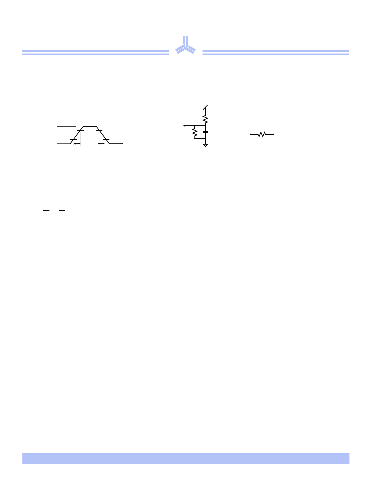
AC test conditions
- Output load: see Figure B
- Input pulse level: GND to VCC See Figure A.
- Input rise and fall times: 2 ns. See Figure A.
- Input and output timing reference levels: 1.5V.
VCC 90%
90%
10%
GND
2 ns
10%
Figure A: Input pulse
+5.0V
Dout
255Ω
480Ω
C10
GND
Figure B: Output load
Thevenin equivalent
168Ω
Dout
+1.72V
Notes
1 During VCC power-up, a pull-up resistor to VCC on CE is required to meet ISB specification.
2 For test conditions, see AC Test Conditions, Figures A, B.
3 These parameters are specified with CL = 5pF, as in Figures B. Transition is measured ±500mV from steady-state voltage.
4 This parameter is guaranteed, but not tested.
5 WE is High for read cycle.
6 CE and OE are Low for read cycle.
7 Address valid prior to or coincident with CE transition Low.
8 All read cycle timings are referenced from the last valid address to the first transitioning address.
9 All write cycle timings are referenced from the last valid address to the first transitioning address.
10 C=30pF, except on High Z and Low Z parameters, where C=5pF.
9/24/04; v.1.2
Alliance Semiconductor
P. 6 of 9
Share Link: 