BU7242SF-E2 데이터 시트보기 (PDF) - ROHM Semiconductor
부품명
상세내역
제조사
BU7242SF-E2
ROHM Semiconductor
BU7242SF-E2 Datasheet PDF : 37 Pages
| |||
BU7261/BU7261S family, BU7241/BU7241S family, BU7295/BU7295S family, BU7275/BU7275S family
BU7262/BU7262S family, BU7242/BU7242S family, BU7264/BU7264S family, BU7244/BU7244S family Technical Note
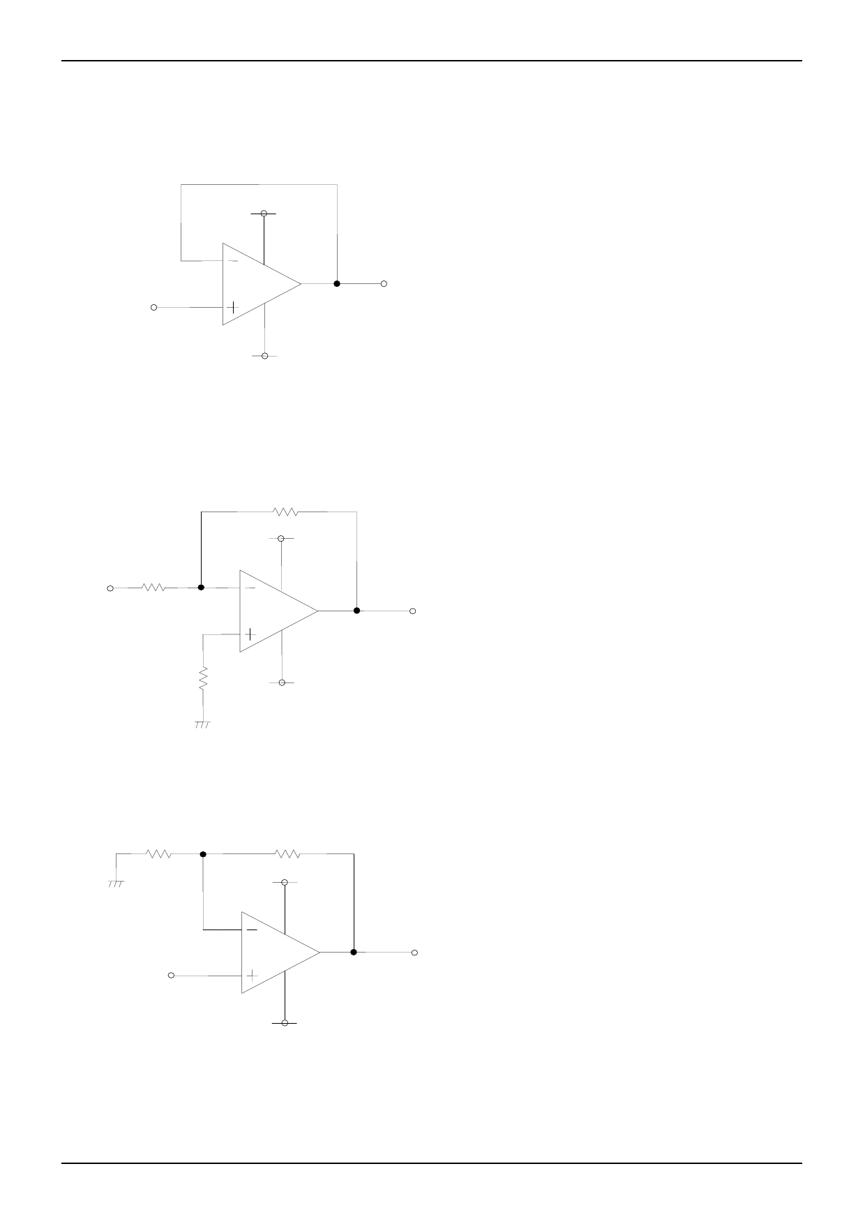
●Examples of circuit
○Voltage follower
VDD
Vout
Vin
VSS
Fig. 190 Voltage follower circuit
○Inverting amplifier
Voltage gain is 0 [dB].
This circuit controls output voltage (Vout) equal input
voltage (Vin), and keeps Vout with stable because of high
input impedance and low output impedance.
Vout is shown next formula.
Vout=Vin
R1
Vin
R2
VDD
R1//R2
VSS
For inverting amplifier, Vin is amplified by voltage gain
decided R1 and R2, and phase reversed voltage is
outputted.
Vout is shown next formula.
Vout
Vout=-(R2/R1)・Vin
Input impedance is R1.
Fig. 191 Inverting amplifier circuit
○Non-inverting amplifier
R1
R2
VDD
Vin
VSS
Fig. 192 Non-inverting amplifier circuit
For non-inverting amplifier, Vin is amplified by voltage
gain decided R1 and R2, and phase is same with Vin.
Vout is shown next formula.
Vout
Vout=(1+R2/R1)・Vin
This circuit realizes high input impedance because Input
impedance is operational amplifier’s input Impedance.
www.rohm.com
© 2010 ROHM Co., Ltd. All rights reserved.
30/36
2010.12 - Rev.A
Share Link: 