CF5017 데이터 시트보기 (PDF) - Nippon Precision Circuits
부품명
상세내역
제조사
CF5017 Datasheet PDF : 10 Pages
| |||
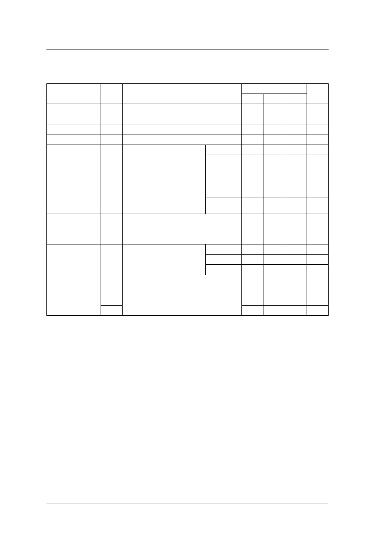
CF5017 series
5V operation (CF5017ALA, ALB, ALC)
VDD = 4.5 to 5.5V, VSS = 0V, Ta = −40 to +85°C unless otherwise noted.
Parameter
Symbol
Condition
HIGH-level output voltage
LOW-level output voltage
HIGH-level input voltage
LOW-level input voltage
Output leakage current
Current consumption
Standby current
INHN pull-up resistance
AC feedback resistance
DC feedback resistance
AC feedback capacitance
Built-in capacitance
VOH Q: Measurement cct 1, VDD = 4.5V, IOH = 16mA
VOL Q: Measurement cct 2, VDD = 4.5V, IOL = 16mA
VIH INHN
VIL INHN
IZ Q: Measurement cct 2, INHN = LOW
VOH = VDD
VOL = VSS
CF5017ALA
f = 40MHz
I DD
Measurement cct 3, load cct 1,
INHN = open, CL = 30pF
CF5017ALB
f = 60MHz
CF5017ALC
f = 80MHz
IST Measurement cct 3, INHN = LOW
RUP1
Measurement cct 4
RUP2
Rf1
Design value. A monitor pattern on a
wafer is tested.
CF5017ALA
CF5017ALB
CF5017ALC
Rf2 Measurement cct 5
Cf Design value. A monitor pattern on a wafer is tested.
CG
Design value. A monitor pattern on a wafer is tested.
CD
Rating
Unit
min
typ
max
3.9
4.2
–
V
–
0.3
0.4
V
0.7V DD
–
–
V
–
–
0.3V DD
V
–
–
10
µA
–
–
10
µA
–
16
32
mA
–
26
52
mA
–
35
70
mA
–
–
10
µA
1
2
4
MΩ
20
100
200
kΩ
2.97
3.5
4.03
kΩ
2.97
3.5
4.03
kΩ
2.97
3.5
4.03
kΩ
50
–
150
kΩ
8.5
10
11.5
pF
6.8
8
9.2
pF
12.7
15
17.3
pF
SEIKO NPC CORPORATION —5
Share Link: 