CY7C1324H-133AXI 데이터 시트보기 (PDF) - Cypress Semiconductor
부품명
상세내역
제조사
CY7C1324H-133AXI Datasheet PDF : 15 Pages
| |||
CY7C1324H
Capacitance[8]
Parameter
Description
CIN
CCLK
CI/O
Input Capacitance
Clock Input Capacitance
Input/Output Capacitance
Thermal Resistance[8]
Parameter
ΘJA
ΘJC
Description
Thermal Resistance
(Junction to Ambient)
Thermal Resistance
(Junction to Case)
Test Conditions
TA = 25°C, f = 1 MHz,
VDD = 3.3V.
VDDQ = 2.5V
Test Conditions
Test conditions follow standard test methods and proce-
dures for measuring thermal impedance, per
EIA/JESD51
100 TQFP
Max.
5
5
5
100 TQFP
Package
30.32
6.85
Unit
pF
pF
pF
Unit
°C/W
°C/W
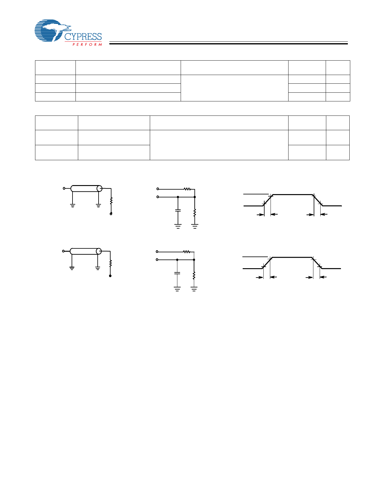
AC Test Loads and Waveforms
3.3V I/O Test Load
OUTPUT
Z0 = 50Ω
3.3V
OUTPUT
RL = 50Ω
5 pF
VL = 1.5V
(a)
INCLUDING
JIG AND
SCOPE
R = 317Ω
R = 351Ω
VDD
GND
ALL INPUT PULSES
10%
90%
≤ 1 ns
90%
10%
≤ 1 ns
(b)
(c)
2.5V I/O Test Load
OUTPUT
Z0 = 50Ω
2.5V
OUTPUT
RL = 50Ω
5 pF
VT = 1.25V
(a)
INCLUDING
JIG AND
SCOPE
R = 1667Ω
R =1538Ω
VDDQ
GND
ALL INPUT PULSES
10%
90%
≤ 1 ns
90%
10%
≤ 1 ns
(b)
(c)
Notes:
8. Tested initially and after any design or process change that may affect these parameters.
Document #: 001-00208 Rev. *B
Page 8 of 15
[+] Feedback
Share Link: 