CY7C63001A-SC 데이터 시트보기 (PDF) - Cypress Semiconductor
부품명
상세내역
제조사
CY7C63001A-SC Datasheet PDF : 31 Pages
| |||
FOR
FOR
CY7C63000A/CY7C63001A
CY7C63100A/CY7C63101A
The clock oscillator, GPIO, and timers restart immediately upon exiting suspend mode. The USB engine and microcontroller return
to a fully functional state no more than 256 µs later. Before servicing any interrupt requests, the microcontroller executes the
instruction following the I/O write that placed the device into suspend mode.
Both the GPIO interrupt and the Cext interrupt allow the USB Controller to wake-up periodically and poll potentiometers, optics,
and other system components while maintaining a very low average power consumption. The Cext Interrupt is preferred for lowest
power consumption.
For Cext to generate an “Instant-on” interrupt, the pin must be connected to ground with an external capacitor and connected to
VCC with an external resistor. A “0” is written to the Cext register located at I/O address 0x22 to discharge the capacitor. Then, a
“1” is written to disable the open-drain output driver. A Schmitt trigger input circuit monitors the input and generates a wake-up
interrupt when the input voltage rises above the input threshold. By changing the values of the external resistor and capacitor,
the user can fine tune the charge rate of the R-C timing circuit. The format of the Cext register is shown in Figure 5-5. Reading
the register returns the value of the Cext pin. During a reset, the Cext pin is HIGH.
b7
Reserved
b6
Reserved
b5
Reserved
b4
Reserved
b3
Reserved
b2
Reserved
b1
Reserved
0
0
0
0
0
0
0
Figure 5-5. The Cext Register (Address 0x22)
b0
CEXT
R/W
1
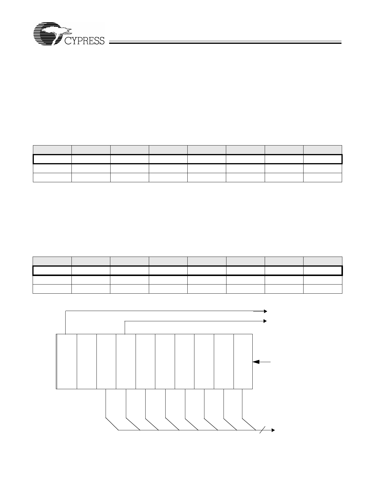
5.5 On-Chip Timer
The USB Controller is equipped with a free-running timer driven by a clock one-sixth the resonator frequency. Bits 0 through 7 of
the counter are readable from the read-only Timer Register located at I/O address 0x23. The Timer Register is cleared during a
Power-On Reset and whenever Suspend mode is entered. Figure 5-6 illustrates the format of this register and Figure 5-7 is its
block diagram.
With a 6 MHz resonator, the timer resolution is 1 µs.
The timer generates two interrupts: the 128-µs interrupt and the 1.024-ms interrupt.
b7
b6
b5
b4
b3
b2
b1
b0
T.7
T.6
T.5
T.4
T.3
T.2
T.1
T.0
R
R
R
R
R
R
R
R
0
0
0
0
0
0
0
0
Figure 5-6. Timer Register (Address 0x23)
1.024-ms interrupt
128-ms interrupt
9
8
7
6
54
32
1
0
Resonator Clock/6
Document #: 38-08026 Rev. **
Figure 5-7. Timer Block Diagram
8
To Timer Register
Page 11 of 31
Share Link: 