CY8C27466 데이터 시트보기 (PDF) - Cypress Semiconductor
부품명
상세내역
제조사
CY8C27466 Datasheet PDF : 39 Pages
| |||
CY8C27x66 Preliminary Data Sheet
1. Pin Information
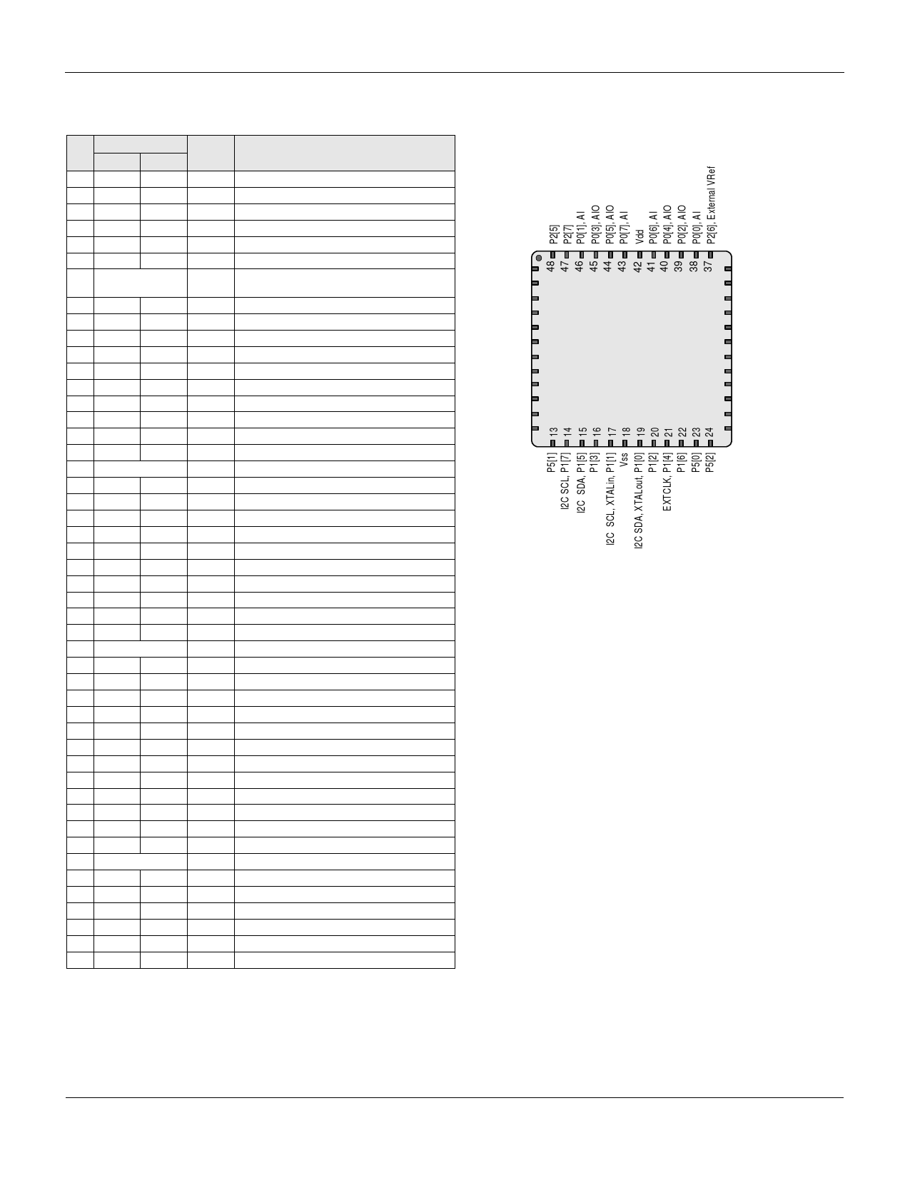
Table 1-4. 48-Pin Part Pinout (MLF*)
Pin
Type
Pin
No. Digital Analog Name
Description
1
IO
I P2[3] Direct switched capacitor block input.
2
IO
I P2[1] Direct switched capacitor block input.
3
IO
P4[7]
4
IO
P4[5]
5
IO
P4[3]
6
IO
P4[1]
7
Power
SMP Switch Mode Pump (SMP) connection to
external components required.
8
IO
P3[7]
9
IO
P3[5]
10
IO
P3[3]
11
IO
P3[1]
12
IO
P5[3]
13
IO
P5[1]
14
IO
P1[7] I2C Serial Clock (SCL)
15
IO
P1[5] I2C Serial Data (SDA)
16
IO
P1[3]
17
IO
P1[1] Crystal (XTALin), I2C Serial Clock (SCL)
18
Power
Vss
Ground connection.
19
IO
P1[0] Crystal (XTALout), I2C Serial Data (SDA)
20
IO
P1[2]
21
IO
P1[4] Optional External Clock Input (EXTCLK)
22
IO
P1[6]
23
IO
P5[0]
24
IO
P5[2]
25
IO
P3[0]
26
IO
P3[2]
27
IO
P3[4]
28
IO
P3[6]
29
Input
XRES Active high pin reset with internal pull down.
30
IO
P4[0]
31
IO
P4[2]
32
IO
P4[4]
33
IO
P4[6]
34
IO
I P2[0] Direct switched capacitor block input.
35
IO
I P2[2] Direct switched capacitor block input.
36
IO
P2[4] External Analog Ground (AGND)
37
IO
P2[6] External Voltage Reference (VREF)
38
IO
I P0[0] Analog column mux input.
39
IO
IO P0[2] Analog column mux input and column output.
40
IO
IO P0[4] Analog column mux input and column output.
41
IO
I P0[6] Analog column mux input.
42
Power
Vdd
Supply voltage.
43
IO
I P0[7] Analog column mux input.
44
IO
IO P0[5] Analog column mux input and column output.
45
IO
IO P0[3] Analog column mux input and column output.
46
IO
I P0[1] Analog column mux input.
47
IO
P2[7]
48
IO
P2[5]
LEGEND: A = Analog, I = Input, and O = Output.
* The MLF package has a center pad that must be connected to the ground (Vss).
CY8C27666 48-Pin PSoC Device
AI, P2[3] 1
AI, P2[1] 2
P4[7] 3
P4[5] 4
P4[3] 5
P4[1] 6
SMP 7
P3[7] 8
P3[5] 9
P3[3] 10
P3[1] 11
P5[3] 12
MLF
(Top View)
36 P2[4], External AGND
35 P2[2], AI
34 P2[0], AI
33 P4[6]
32 P4[4]
31 P4[2]
30 P4[0]
29 XRES
28 P3[6]
27 P3[4]
26 P3[2]
25 P3[0]
June 1, 2004
Document No. 38-12019 Rev. *B
11
Share Link: 