ECH8659 데이터 시트보기 (PDF) - SANYO -> Panasonic
부품명
상세내역
제조사
ECH8659 Datasheet PDF : 7 Pages
| |||
ECH8659
Electrical Characteristics at Ta=25°C
Parameter
Symbol
Drain-to-Source Breakdown Voltage
Zero-Gate Voltage Drain Current
Gate-to-Source Leakage Current
Cutoff Voltage
Forward Transfer Admittance
Static Drain-to-Source On-State Resistance
Input Capacitance
Output Capacitance
Reverse Transfer Capacitance
Turn-ON Delay Time
Rise Time
Turn-OFF Delay Time
Fall Time
Total Gate Charge
Gate-to-Source Charge
Gate-to-Drain “Miller” Charge
Diode Forward Voltage
V(BR)DSS
IDSS
IGSS
VGS(off)
| yfs |
RDS(on)1
RDS(on)2
RDS(on)3
Ciss
Coss
Crss
td(on)
tr
td(off)
tf
Qg
Qgs
Qgd
VSD
Conditions
ID=1mA, VGS=0V
VDS=30V, VGS=0V
VGS=±16V, VDS=0V
VDS=10V, ID=1mA
VDS=10V, ID=3.5A
ID=3.5A, VGS=10V
ID=2A, VGS=4.5V
ID=2A, VGS=4V
VDS=10V, f=1MHz
VDS=10V, f=1MHz
VDS=10V, f=1MHz
See specified Test Circuit.
VDS=15V, VGS=10V, ID=3.5A
IS=7A, VGS=0V
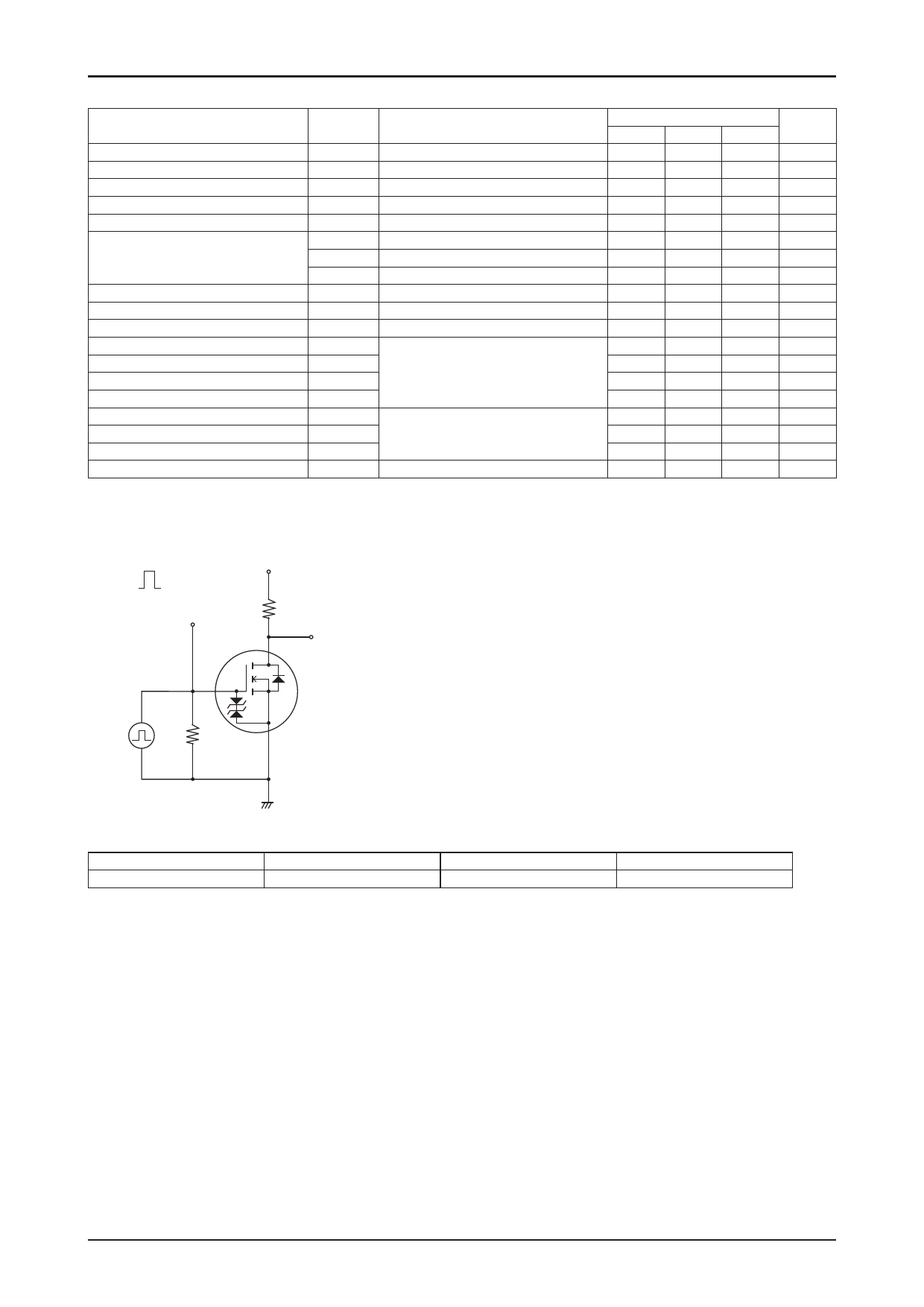
Switching Time Test Circuit
VIN
10V
0V
VIN
PW=10μs
D.C.≤1%
G
VDD=15V
ID=3.5A
RL=4.3Ω
D
VOUT
ECH8659
P.G
50Ω
S
Ratings
Unit
min
typ
max
30
V
1
μA
±10
μA
1.2
2.6
V
2.2
3.7
S
18
24 mΩ
29
41 mΩ
39
55 mΩ
710
pF
120
pF
72
pF
10
ns
25
ns
43
ns
25
ns
11.8
nC
2.4
nC
2.0
nC
0.79
1.2
V
Ordering Information
Device
ECH8659-TL-H
Package
ECH8
Shipping
3,000pcs./reel
memo
Pb Free and Halogen Free
No. A1224-2/7
Share Link: 